Cover tape for packaging semiconductor device and package for semiconductor device

a technology for packaging semiconductor devices and packaging, applied in the directions of transportation and packaging, semiconductor/solid-state device details, containers, etc., can solve the problems of two to three times slower mounting speed of the tray, difficult embossed tape transportation, and inability to achieve high-precision processing

Inactive Publication Date: 2011-10-11
SOCIONEXT INC
View PDF27 Cites 2 Cited by
  • Summary
  • Abstract
  • Description
  • Claims
  • Application Information

AI Technical Summary

Benefits of technology

[0016]Since the cover tape for packaging semiconductor device has the net-like structure at least in a portion, the contact area with the semiconductor device is decreased because of the multiple airspaces provided by the net-like structure and the airspaces exhibit ventilation function enabling to inhibit the popping out of the semiconductor devices caused by absorption at low pressure and static electricity, etc. which occurs during high-speed transportation and high-speed peeling. Therefore, the cover tape for packaging semiconductor device can ensure quality and reliability of a semiconductor device, is capable of improving the mounting speed of the semiconductor device by shipment in tape and can be suitably used for shipment in tape of small-size package, particularly small, thin and light electronic components such as CSP / CHIP.
[0018]Since the package for semiconductor device uses the cover tape for packaging semiconductor device of the present invention, it is possible to transport the semiconductor device while ensuring its quality and reliability and the package for semiconductor device can be suitably used for high-speed transportation of the electronic components such as the semiconductor device by shipment in tape.

Problems solved by technology

However, with a progress of polarization (grow in size and downsizing) of semiconductor devices, small, thin and light electronic components such as CSP / CHIP, etc. are being shipped or mounted in tray because shipment in embossed tape is difficult due to manufacturing of the embossed tape which makes the high-precision processing impossible.
The shipment in tray has a problem in mounting speed which is two to three times slower compared to that of the shipment in tape because of the delay caused by the use of intermediate table when a general-purpose mounting device is used.
The mounting device of high-speed type has a problem that it is not applicable for shipment in tray.

Method used


Image

  • Cover tape for packaging semiconductor device and package for semiconductor device
  • Cover tape for packaging semiconductor device and package for semiconductor device
  • Cover tape for packaging semiconductor device and package for semiconductor device

Examples


first embodiment

[0032]The first embodiment of the cover tape for packaging semiconductor device of the present invention will be explained referring to figures below.

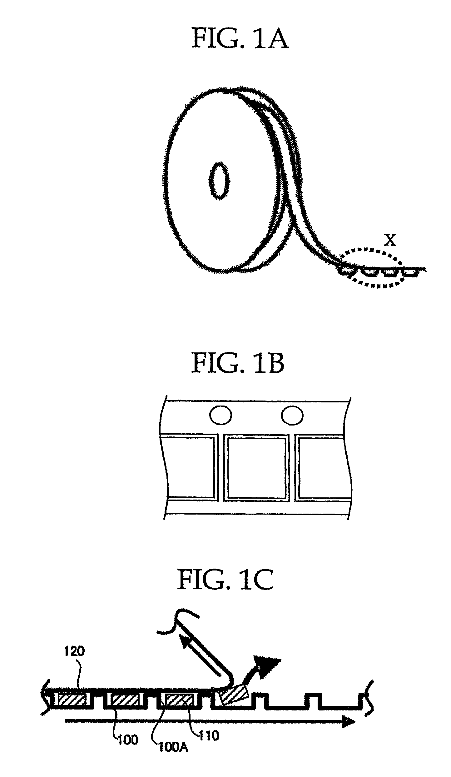
[0033]FIG. 2A is a perspective view showing the cover tape for packaging semiconductor device of the present invention in the first embodiment.

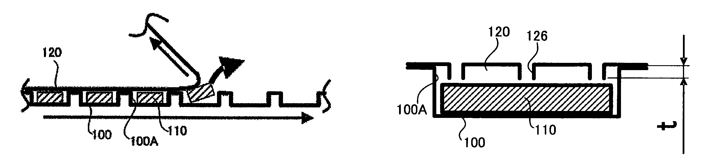
[0034]A cover tape 10 as shown in FIG. 2A is pasted on the embossed tape for use. The embossed tape is not particularly limited and may be selected from known embossed tapes accordingly. Examples include an embossed tape 100 as shown in FIG. 1C on which pockets (concave portions) 100A are formed at regular intervals in a length direction for containing semiconductor devices (IC chips 110, for example). The cover tape 10 prevents dropout of semiconductor devices (IC chips 110, for example) contained in the pockets 100A on the embossed tape 100 when pasted on the embossed tape 100. Furthermore, the cover tape 10 is shipped and transported as wound on reels with the embossed tape 100 (FIG. 1A). The...


PUM


Abstract

The present invention provides a cover tape for packaging a semiconductor device which protects the outer shape of the semiconductor device, and is capable of improving the mounting speed of the semiconductor device by shipment in tape, and a package for the semiconductor device using the cover tape for packaging the semiconductor device. The cover tape for packaging the semiconductor device has a net-shaped structure at least in a portion, and the cover tape for packaging the semiconductor device is pasted onto an embossed tape which has a number of pockets containing semiconductor devices. The package for the semiconductor device contains an embossed tape which has a number of pockets which contain semiconductor devices, and the cover tape for packaging the semiconductor device.

Description

CROSS-REFERENCE TO RELATED APPLICATIONS[0001]This application is based upon and claims the benefits of the priority from the prior Japanese Patent Application No. 2006-073586, filed on Mar. 16, 2006, the entire contents of which are incorporated herein by reference.BACKGROUND OF THE INVENTION[0002]1. Field of the Invention[0003]The present invention relates to a cover tape for packaging semiconductor device which ensures quality and reliability of a semiconductor device by protecting the outer shape of the semiconductor device, and is capable of improving the mounting speed of the semiconductor device by shipment in tape, and a package for semiconductor device using the cover tape for packaging semiconductor device.[0004]2. Description of the Related Art[0005]The shipment in embossed tape has been employed as a delivering embodiment of a semiconductor device for mounting the semiconductor device on a substrate. In the shipment in embossed tape, the semiconductor device is delivered ...

Claims


Application Information

Patent Timeline
Patent Type & Authority Patents(United States)
IPC IPC(8): B65D85/00H01L23/02
CPCH01L21/67356H01L21/6835H05K13/0084H01L2221/68313H01L2924/19041
Inventor SASAMURA, KEIICHIYAZAKI, KENICHIHAMANAKA, YUUZOUANDO, YUKIOHASHIBA, HIDEYASU
Owner SOCIONEXT INC
Why Eureka
Try Eureka