Method of manufacturing mount structure without introducing degraded bonding strength of electronic parts due to segregation of low-strength/low-melting point alloy

a technology of low-strength/low-melting point alloy and manufacturing method, which is applied in the manufacture of final products, manufacturing tools, metal working equipment, etc., can solve the problems of adversely affecting the earth environment, inability to withstand high temperature, and difficulty in using mounting apparatus and mounting method for use with sn, so as to ensure the quality and reliability of solder-based bonding

Inactive Publication Date: 2005-07-12
NEC PERSONAL COMPUTERS LTD
View PDF65 Cites 0 Cited by
  • Summary
  • Abstract
  • Description
  • Claims
  • Application Information

AI Technical Summary

Benefits of technology

[0023]It is an object of the present invention to provide a method of manufacturing a mount structure which is capable of preventing the formation of a low-strength / low-melting point alloy layer near the interfaces between a land and a solder to sufficiently ensure the quality and reliability of solder-based bonding, and the mount structure.
[0025]In this way, the solder paste can be solidified in a uniform composition before a low-strength / low-melting point alloy segregates in regions around interfaces between lands and solders on the printed board. This can suppress the formation of low-strength / low-melting point alloy layers in regions around interfaces between lands and solders on the printed board, and ensure the quality and reliability of the solder-based bonding. For example, when an Sn—Zn—Bi based alloy is used as the solder paste, from a viewpoint of improvement on the wettability of a Pb-free Sn—Zn based solder, for soldering an electronic part having leads covered with a plating film containing Pb, it is possible to prevent the segregation of Sn—Zn—Pb (the melting point of which is 177° C.) and Sn—Pb—Bi (the melting point of which is 98° C.).
[0026]When an Sn—Zn—Bi based alloy containing 3% or less of Bi is used as the solder paste, it is possible to further suppress the segregation of Sn—Pb—Bi. In addition, the flexibility of the Sn—Pb—Bi based solder can be increased when it contains less than 3 wt % of Bi, so that it is also possible to improve the endurance to environmental changes such as the ambient temperature.
[0027]Also, When two or more kinds of solder powders are blended into a solder paste for use in the present invention, the resulting solder paste exhibits a larger temperature difference between the liquidus and solidus, thereby making it possible to suppress the chip build-up defect.
[0028]For conducting a double-sided reflow process including a first reflow step on one side of a printed board and a second reflow step on the other side of the printed board, solders on both sides of the printed board are forcedly cooled down and solidified from a melted state at a cooling speed of 1.5° C. / second or higher. In this event, the segregation of Sn—Zn—Pb and Sn—Pb—Bi is prevented in regions around interfaces of lands and solders on the one side of the printed board on which electronic parts have been previously mounted by the first reflow step, even after the printed board has undergone the second reflow step, thereby making it possible to ensure the quality and reliability of the solder-based bonding.
[0029]For conducting a reflow / flow composite process including a reflow step on one side of a printed board and a flow step on the other side of the printed board, the flow processing is performed during the flow step while a solder on the one side of the printed circuit board is maintained at temperatures of 170° C. or lower. In this event, Sn—Zn—Pb formed in very small quantities in the reflow step can be prevented from melting again during the flow step on the one side of the printed board on which electronic parts have been previously mounted by the reflow step. It is therefore possible to ensure the quality and reliability of the solder-based bonding on the one side of the print board even after the printed board has undergone the flow step.

Problems solved by technology

Electronic parts which cannot withstand the high temperature in the furnace for the aforementioned reflow processing, electronic parts which are mounted through the flow processing with difficulties are manually soldered after the flow processing is terminated.
However, this Sn—Pb based solder contains Pb, a poisonous heavy metal, which adversely affects the earth environment if devices are not appropriately disposed after use.
However, the Sn—Ag based solder has a melting point at slightly lower than 220° C. which is higher than the melting point of the Sn—Pb based solder, i.e., approximately 183° C. This higher melting point makes it difficult to utilize a mounting apparatus and a mounting method for use with the Sn—Pb based solder as they are.
Therefore, the use of the Sn—Ag based solder for mounting a variety of electronic parts implies a problem that the electronic parts are required to withstand higher temperatures.
However, the aforementioned Sn—Zn based solder has a problem of high susceptibility of Zn to oxidization, and poor wettability, as compared with the conventionally used Sn—Pb based solder.
This causes difficulties in ensuring the soldering quality and reliability similar to before if electronic parts are mounted by the Sn—Zn based solder using conventional facilities and mounting method.
Consequently, the low-strength / low-melting point alloy layers in these interface regions adversely affect the mounting quality and reliability.
This causes a higher susceptibility to partial delamination or complete failure in bonding of electronic parts in the interface regions when a PCB is bowed or twisted.

Method used


Image

  • Method of manufacturing mount structure without introducing degraded bonding strength of electronic parts due to segregation of low-strength/low-melting point alloy
  • Method of manufacturing mount structure without introducing degraded bonding strength of electronic parts due to segregation of low-strength/low-melting point alloy
  • Method of manufacturing mount structure without introducing degraded bonding strength of electronic parts due to segregation of low-strength/low-melting point alloy

Examples


first embodiment

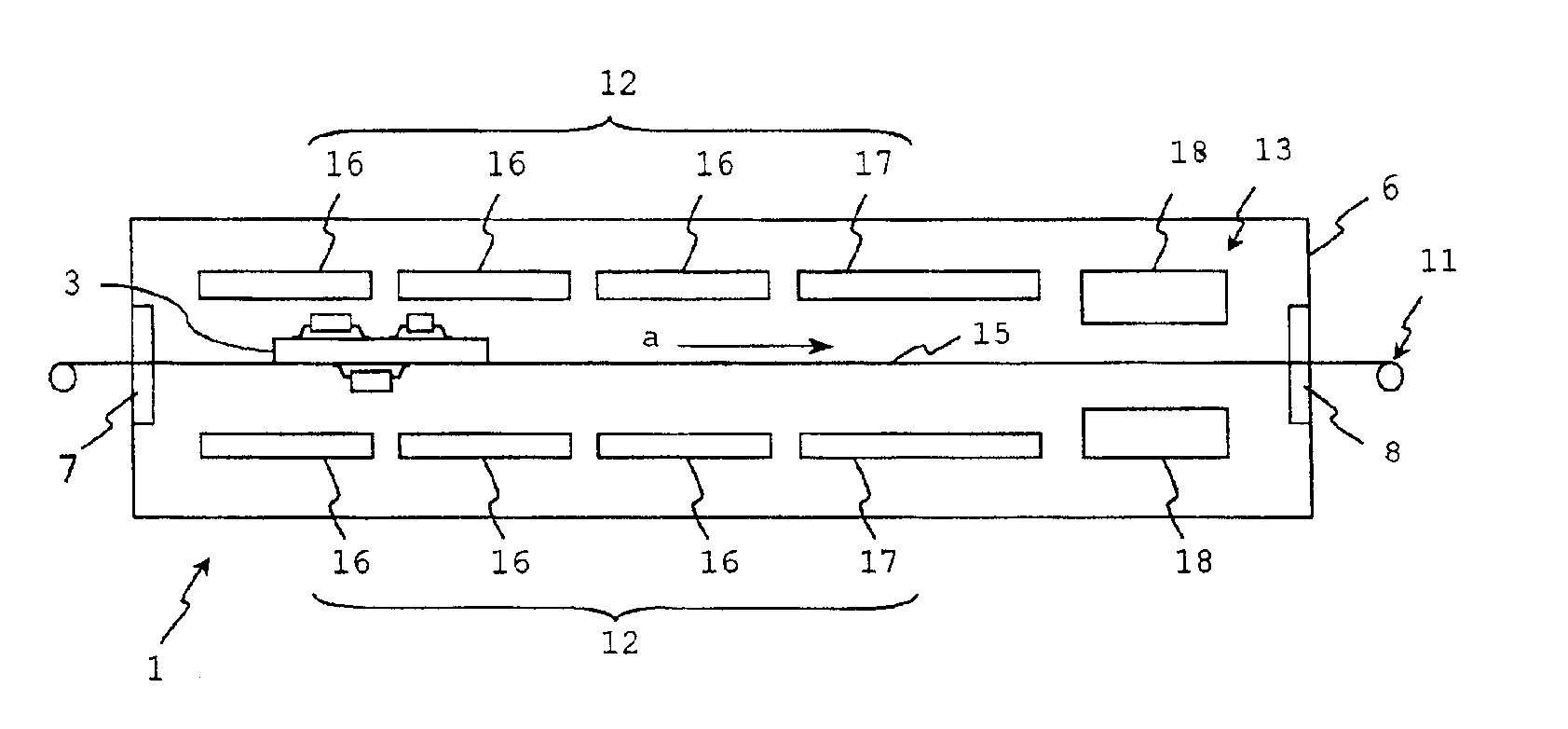
[0050]In a first embodiment, a mount structure is manufactured by a double-sided reflow process for soldering electronic parts on both sides of a PCB by reflowing.

[0051]A reflow apparatus for use in the reflow processing according to the first embodiment applies the reflow processing to a PCB which has a variety of electronic parts mounted on a solder paste printed on lands in a preceding step. The reflow apparatus employs an Sn—Zn—Bi based alloy, which is an Sn—Zn based alloy containing Bi, as the solder paste. An electronic part having leads covered with a plating film containing Pb is used as one of the electronic parts mounted on the PCB.

[0052]As illustrated in FIG. 3, reflow apparatus 1 for use in the reflow processing according to the first embodiment comprises furnace 6 for performing the reflow processing on PCB 3. Furnace 6 is provided with an inlet port 7 at one end side for introducing PCB 3 subjected to the reflow processing, and an outlet port 8 on the other end side fo...

second embodiment

[0096]In a second embodiment, a mount structure is manufactured by a reflow / flow composite process for soldering electronic parts by reflowing on one side of PCB 3 and subsequently soldering electronic parts by flowing on the other side of PCB 3.

[0097]A flow apparatus for use in the flow processing according to the second embodiment applies the flow processing to a PCB which has throughholes through which leads of a variety of electronic parts are inserted to load the electronic parts on the PCB. As a solder for use in the flow processing, an Sn—Ag based alloy, an Sn—Cu based alloy, an Sn—Zn based alloy and the like are preferably used from a viewpoint Pb-free promotion. Also, used as electronic parts mounted on the PCB are those electronic parts which have leads covered with a plating film containing Pb.

[0098]As illustrated in FIG. 7, flow apparatus 20 for use in the flow processing according to the second embodiment comprises a furnace 21 for performing the flow processing on PCB ...


PUM

PropertyMeasurementUnit
temperaturesaaaaaaaaaa
melting pointaaaaaaaaaa

Abstract

A method of manufacturing a mount structure according to the present invention which forcedly cools down a melted solder paste on a printed circuit board at a cooling speed of 1.5° C. / second or higher to solidify the solder paste when an electronic part is mounted on the printed circuit board by reflow processing.

Description

BACKGROUND OF THE INVENTION[0001]1. Field of the Invention[0002]The present invention relates to a method of manufacturing a mount structure having a variety of electronic parts mounted on a printed circuit board (hereinafter called the PCB) by soldering, and to a mount structure, and more particularly, to a method of manufacturing a mount structure having electronic parts soldered on at least one side of a PCB by reflowing, and to a mount structure.[0003]2. Description of the Prior Art[0004]Conventionally, soldering has been used for mounting a variety of electronic parts on a PCB. In the following, a method of mounting electronic parts using soldering will be described below with reference to the drawings.[0005]Referring first to FIGS. 1A-1F, description will be made on an example of double-sided reflow process for soldering electronic parts on both sides of a PCB by reflowing.[0006]First, solder paste 81 is printed on a land (not shown) of PCB 80 using a printing mask (not shown)...

Claims


Application Information

Patent Timeline
Patent Type & Authority Patents(United States)
IPC IPC(8): H05K3/34
CPCH05K3/3415H05K3/3494H05K3/3463H05K3/3468H05K3/3484Y10T29/53174H05K2203/081H05K2203/1121H05K2203/1476H05K2203/1572H05K2201/062H05K3/3485Y02P70/50H05K3/34
Inventor WATANABE, SHINJISAKAI, HIROSHISUZUKI, MOTOJIIGARASHI, MAKOTOTANAKA, AKIHIRO
Owner NEC PERSONAL COMPUTERS LTD
Why Eureka
Try Eureka