Semiconductor-dielectric-semiconductor device structure fabricated by wafer bonding

a semiconductor and dielectric technology, applied in the direction of semiconductor devices, basic electric elements, electrical equipment, etc., can solve the problems of gate dielectrics, not necessarily very fast operation, and complex technology, and achieve the effect of increasing the control of the dielectric-electrode interfa

Inactive Publication Date: 2006-02-16
ELPIS TECH INC
View PDF17 Cites 74 Cited by
  • Summary
  • Abstract
  • Description
  • Claims
  • Application Information

AI Technical Summary

Benefits of technology

[0013] The present invention provides a method of producing, at least partially, a gate stack of a semiconductor-dielectric-semiconductor device such as a MOSFET or a floating gate memory in which wafer bonding is employed. The present invention thus provides a method for providing increased control over the diel

Problems solved by technology

As MOSFET devices, e.g., insulated-gate field effect transistors, are being scaled down, the technology becomes more complex and new methods are needed to maintain the expected performance enhancement from one device generation to the next.
Gate dielectrics are one of the main problems for field effect device scaling.
Therefore, doped Si may continue to be used, in particular for low power device applications that require low gate leakage, but not necessarily very fast operation.
The situation is even more problematic for field effect devices based on semiconductors other than Si, e.g., Ge, GaAs, etc.
Up to now, no reliable high-quality gate dielectric has been found.
In particular, oxidation of these materials results in poor quality oxide layers that may even be water soluble, as is the case for most germanium oxide phases.
Also deposited metal oxides with sufficient quality have not yet been demonstrated on alternative substrates.
Such results remain singular and are not fully understood.
But even in the potentially simpler case of Si-based MOSFETs, not all issues with high-k implementation have been resolved, despite intense research and development activities in many laboratories worldwide.
This renders such devices unusable for integration.
While there may be some hope to find a better capping layer or to investigate in more detail the

Method used


Image

  • Semiconductor-dielectric-semiconductor device structure fabricated by wafer bonding
  • Semiconductor-dielectric-semiconductor device structure fabricated by wafer bonding

Examples


Embodiment Construction

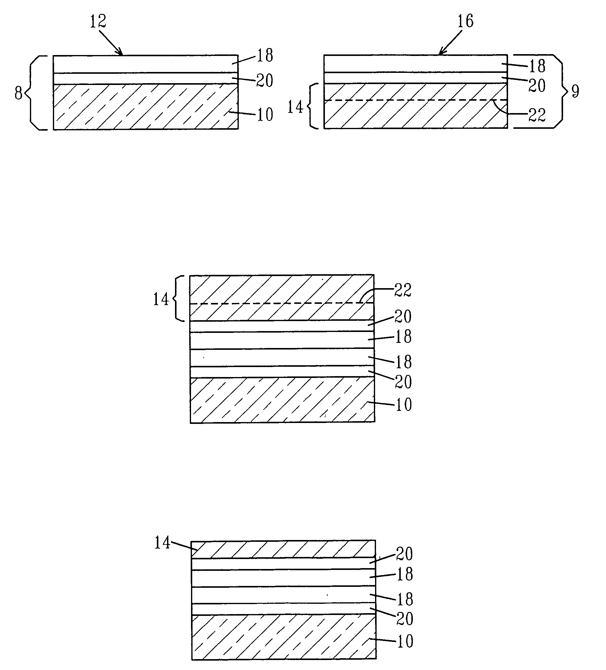
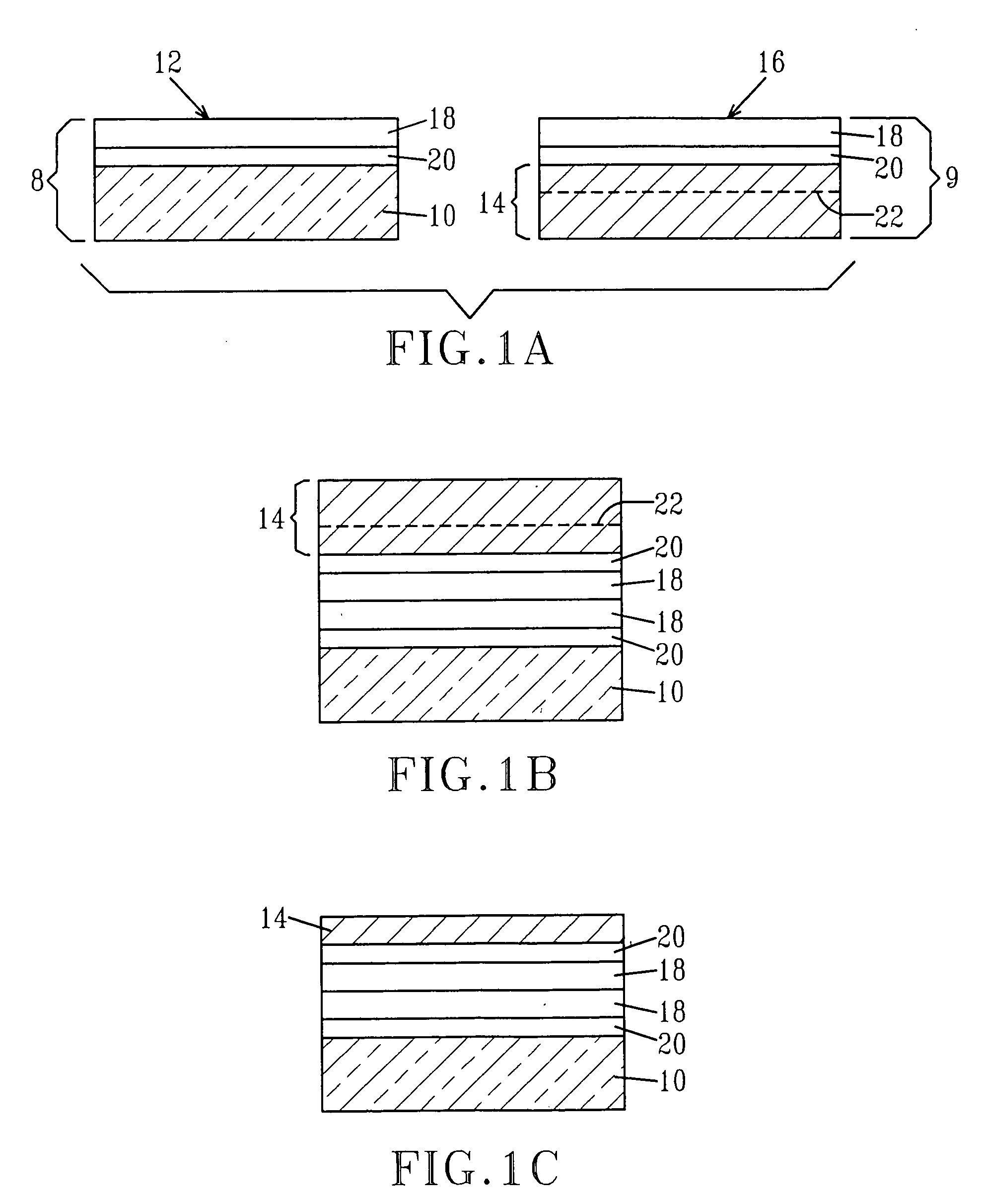
[0024] The present invention, which provides a method of forming a gate stack structure by wafer bonding, will now be described in greater detail by referring to the drawings that accompany the present application. It is noted that the accompanying drawings are not drawn to scale and that like and / or corresponding elements shown in the drawings are referred to by like reference numerals.

[0025] Reference is first made to FIG. 1A which depicts a first structure 8 having a major surface 12 and a second structure 9 having a major surface 16 that can be used in the present invention. In accordance with the present invention, at least one of the first structure 8 or the second structure 9 contains a dielectric material 18 that has a dielectric constant that is greater than silicon dioxide (hereinafter ‘high-k dielectric’18). In the embodiment illustrated, both the first structure 8 and the second structure 9 contain the high-k dielectric 18 formed atop an optional native dielectric layer...


PUM


Abstract

A method of forming a gate stack for semiconductor electronic devices utilizing wafer bonding of at least one structure containing a high-k dielectric material is provided. The method of the present invention includes a step of first selecting a first and second structure having a major surface respectively. In accordance with the present invention, at least one, or both, of the first and second structures includes at least a high-k dielectric material. Next, the major surfaces of the first and second structures are bonded together to provide a bonded structure containing at least the high-k dielectric material of a gate stack.

Description

FIELD OF THE INVENTION [0001] The present invention relates to semiconductor electronic devices and systems and more particularly, to a method of fabricating, at least partially, a gate stack of a semiconductor-dielectric-semiconductor device structure such as, for example, a metal oxide semiconductor field effect transistor (MOSFET) or a floating gate memory. The method of the present invention allows for the fabrication of gate stack structures that are difficult to fabricate using prior art techniques which permits for improved properties and higher performance in field effect devices. BACKGROUND OF THE INVENTION [0002] Today's integrated circuits include a vast number of electronic devices. Smaller devices are a key to enhance device performance and improve reliability. As MOSFET devices, e.g., insulated-gate field effect transistors, are being scaled down, the technology becomes more complex and new methods are needed to maintain the expected performance enhancement from one de...

Claims


Application Information

Patent Timeline
IPC IPC(8): H01L21/3205H01L21/4763
CPCH01L21/76254H01L29/517H01L29/495H01L21/823828
Inventor FRANK, MARTIN M.REZNICEK, ALEXANDERGOUSEV, EVGENI P.CARTIER, EDUARD A.
Owner ELPIS TECH INC
Why Eureka
Try Eureka