

Circuit board structure and fabrication method thereof
a technology of circuit board and dielectric layer, which is applied in the direction of transportation and packaging, chemical apparatus and processes, and applications of non-metallic protective coatings. it can solve the problems of difficult control of the roughening process, the circuit layer can easily detach from the dielectric layer, and the roughening process becomes much more difficult. , to achieve the effect of preventing the formation of excessive roughness, reducing the formation of rough surfaces, and increasing the bonding force of the dielectric layer
- Summary
- Abstract
- Description
- Claims
- Application Information
AI Technical Summary
Benefits of technology
Problems solved by technology
Method used
Image

Examples
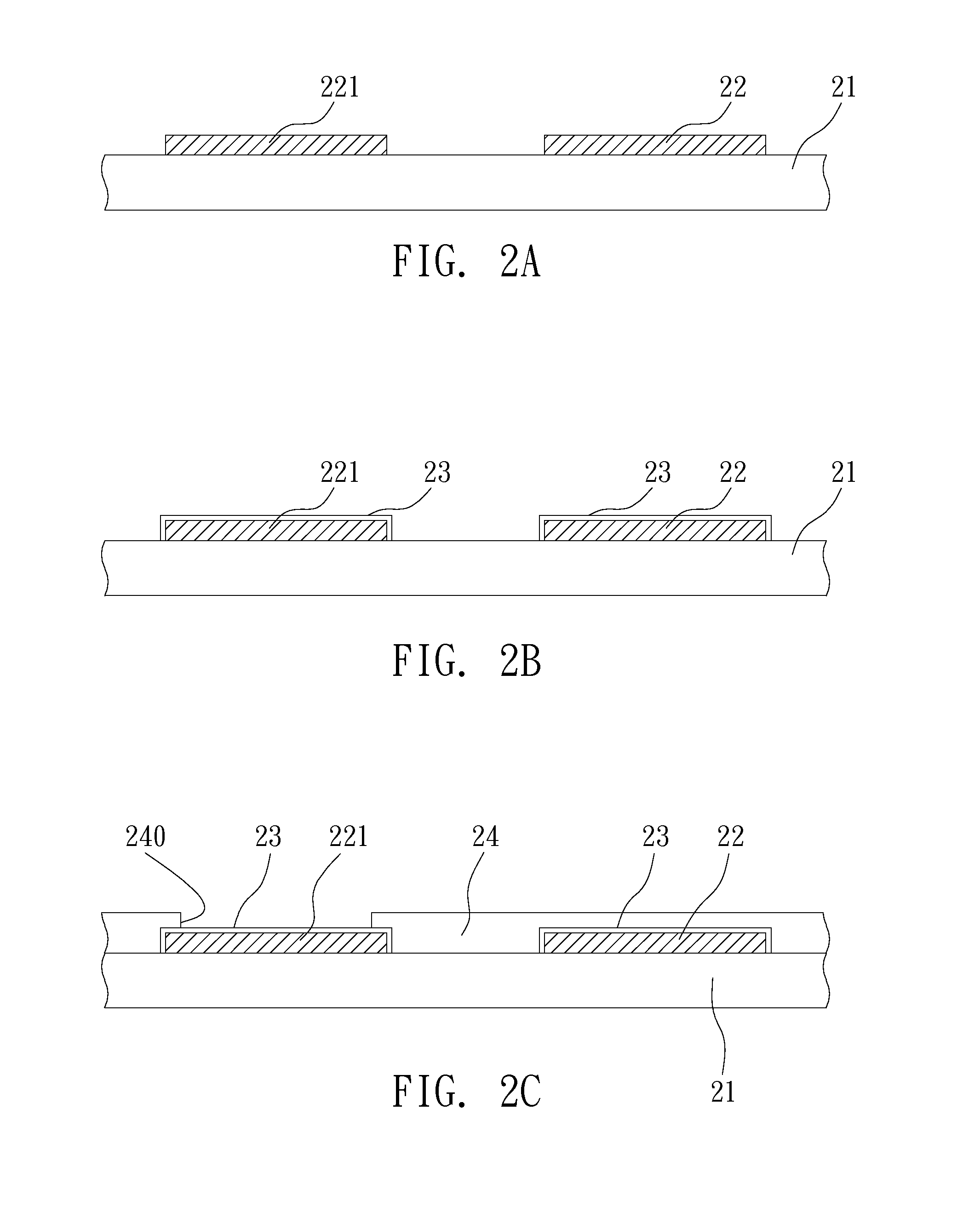
first embodiment
[0024]FIGS. 2A to 2C are cross-sectional views showing a fabrication method of a circuit board structure according to the first embodiment of the present invention.
[0025]Referring to FIG. 2A, a circuit board 21 is provided. The circuit board 21 is a single-layer or multi-layer circuit board required for a front-end circuit process. The circuit board 21 has a circuit layer 22 thereon. The circuit layer 22 comprises a plurality of electrically connecting pads 221 (or known as electrically connecting lands 221). The circuit layer 22 is made of Au, Ag, Cu, Fe, Pd, Pb, Sn, Bi, Sb, Zn, Ni, Zr, Mg, In, Te, or Ga.
[0026]Referring to FIG. 2B, a reactant 23 is formed on the circuit board 21, the reactant 23 formed being limited to the surface of a circuit layer 22, wherein the reactant 23 is an organic metallic polymer with a polymer end and a metal ion end. The polymer end is bonded to the surface of the circuit board 21 by a chemical bond. The metal ion end of the reactant 23 can be bonded t...
second embodiment
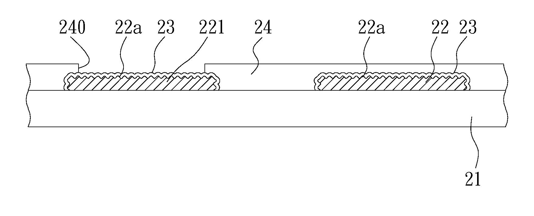
[0031]FIGS. 3A to 3D are cross-sectional views showing a fabrication method of a circuit board structure according to the second embodiment. The second embodiment differs from the first embodiment in that the second embodiment further discloses performing micro-etch pretreatment on the circuit layer.
[0032]Referring to FIG. 3A, a circuit board 21 with a circuit layer 22 thereon is provided. The circuit layer 22 has a plurality of electrically connecting pads 221 (or known as electrically connecting lands 221).
[0033]As shown in FIG. 3B, micro-etch pretreatment is performed on the surface of the circuit layer 22 so as to form a micro-rough surface 22a on the circuit layer 22. The micro-rough surface 22a is a fine, rough surface.
[0034]As shown in FIG. 3C, a reactant 23 is formed on the circuit layer 22, the reactant 23 formed being limited to the surface of a circuit layer 22, wherein the reactant 23 has a polymer end and a metal ion end. The polymer end can be bonded to the surface of ...
PUM
| Property | Measurement | Unit |
|---|---|---|
| bonding force | aaaaa | aaaaa |
| dielectric | aaaaa | aaaaa |
| density | aaaaa | aaaaa |
Abstract
Description
Claims
Application Information