Method of producing semiconductor device

a semiconductor device and semiconductor technology, applied in the direction of semiconductor devices, basic electric elements, electrical appliances, etc., can solve the problems of difficult burying of trenches by hdp-cvd method, unfavorable processing, and affecting so as to promote the removal of seams and improve the yield of semiconductor devices

Active Publication Date: 2008-02-28
MICRON TECH INC
View PDF7 Cites 20 Cited by
  • Summary
  • Abstract
  • Description
  • Claims
  • Application Information

AI Technical Summary

Benefits of technology

[0041]According to the present invention, a stress exerted on seams in the deposited film is controlled to promote the removal of the seams in the annealing step. For this reason, a problem resulting from seams in the deposited film is solved

Problems solved by technology

However, further miniaturization of a device has increased the aspect ratio of a trench, which has made it difficult to bury trenches by the HDP-CVD method.
The etching rate of wet etching to seams SE is higher than that to other portions of the film, which is unfavorable for processing.
However, seams SE cannot be completely removed by suc

Method used


Image

  • Method of producing semiconductor device
  • Method of producing semiconductor device
  • Method of producing semiconductor device

Examples


Embodiment Construction

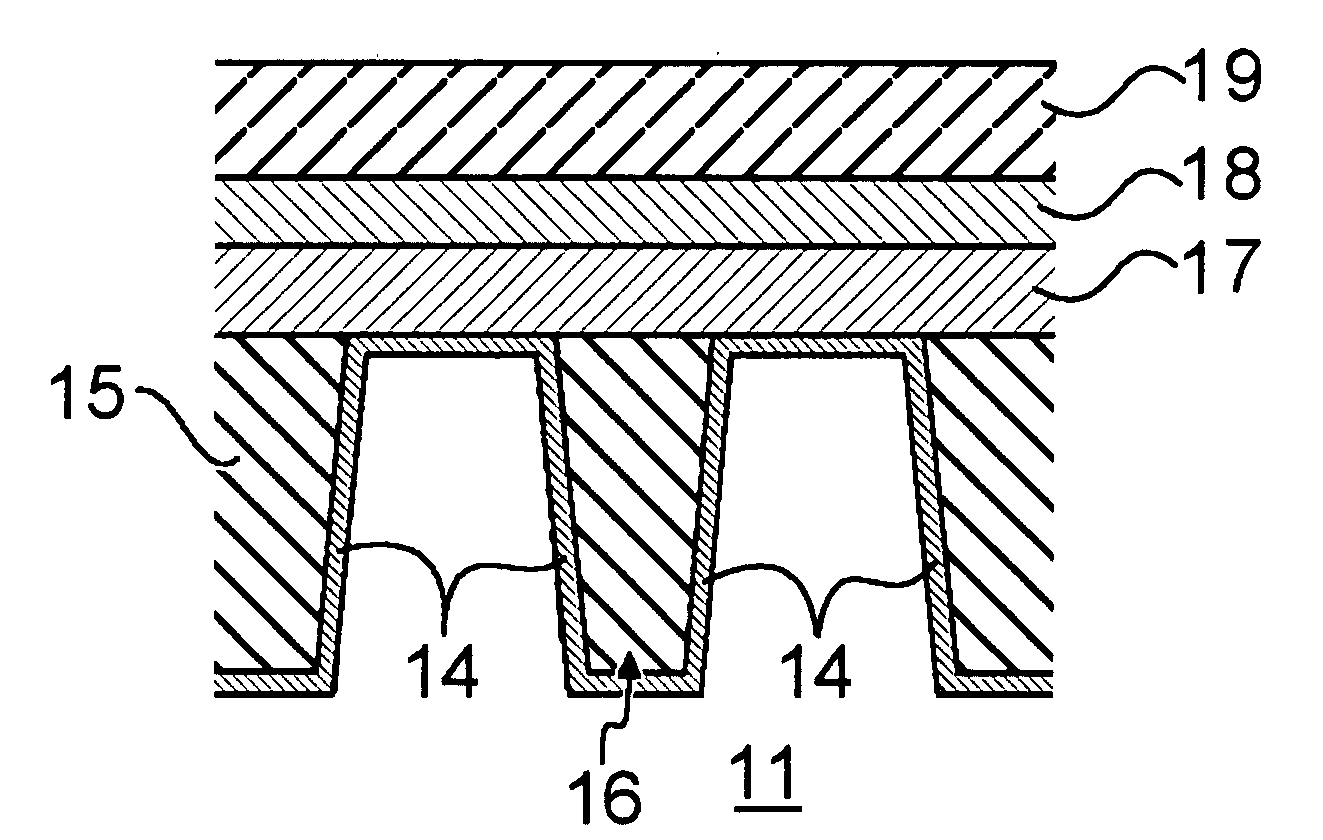
[0047]A method of producing a semiconductor device according to an exemplary embodiment is described below with reference to FIGS. 3A to 3D and FIGS. 4A to 4E.

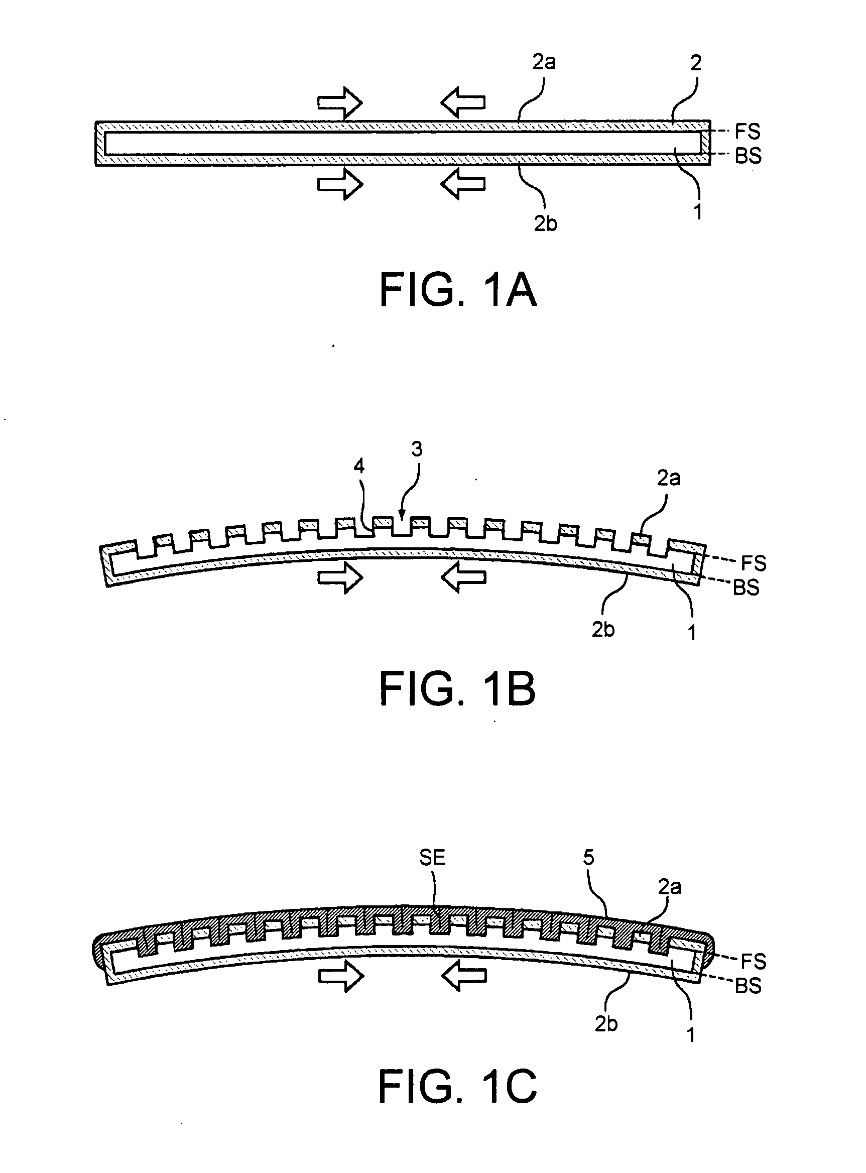
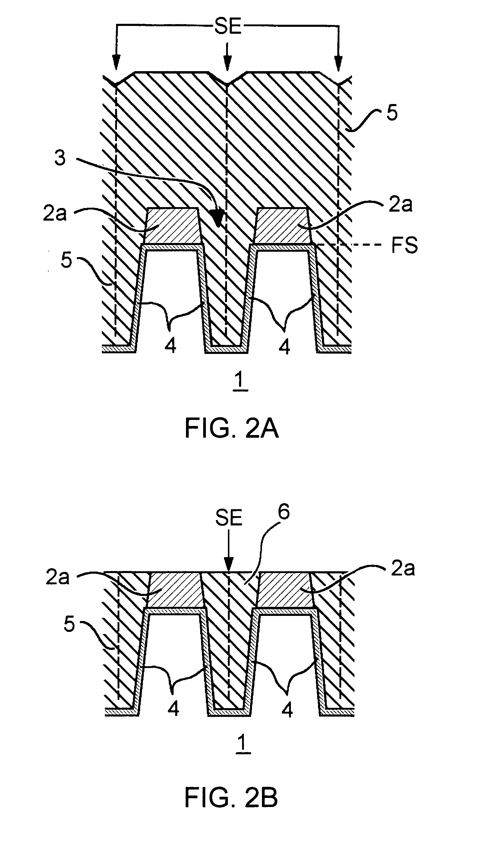
[0048]First, an oxide film (not shown) is formed on semiconductor substrate (semiconductor wafer) 11 by a thermal oxidation process. Then, silicon nitride film (SiN film) 12 is formed by an LP-CVD method. At this point, SiN film 12 is deposited on both sides of semiconductor substrate 11 as illustrated in FIG. 3A. That is to say, on front surface FS of semiconductor substrate 11 is formed SiN film 12a, and on back surface BF of semiconductor substrate 11 is formed SiN film 12b. SiN film 12 exerts a strong tensile stress on semiconductor substrate 11. However, the stress is in balance between front surface FS and back surface BS in the phase illustrated in FIG. 3A, so that “warpage” is not generated on semiconductor substrate 11.

[0049]A mask is formed from SiN film 12a on front surface FS of semiconductor substrate 11 through p...


PUM


Abstract

A method of producing a semiconductor device according to the present invention comprises steps of:
    • (A) forming trenches (13) on the front surface (FS) of a semiconductor substrate (11) on the back surface (BS) of which a nitride film (12b) is formed;
    • (B) depositing an insulating film (15) to bury the trenches (13);
    • (C) removing the nitride film (12b) on the back surface (BS) of the semiconductor substrate (11) after the step (B); and
    • (D) annealing before the insulating film (15) is etched after the step (C).

Description

[0001]This application is based upon and claims the benefit of priority from Japanese patent application No. 2006-226250, filed on Aug. 23, 2006, the disclosure of which is incorporated herein in its entirety by reference.BACKGROUND OF THE INVENTION[0002]1. Field of the Invention[0003]The present invention relates to a method of producing a semiconductor device, and particularly, to a method of producing a semiconductor device comprising device isolation structure.[0004]2. Related Art[0005]There has been known a shallow trench isolation (STI) as device isolation structure in a semiconductor device. The STI structure is formed such that an insulating film is deposited on a semiconductor substrate in which trenches are formed to bury the trenches with the insulating film. A chemical vapor deposition (CVD) method is generally used to deposit the insulating film.[0006]Hitherto, an insulating film has been deposited by a high-density plasma (HDP) CVD method, for example. However, further...

Claims


Application Information

Patent Timeline
IPC IPC(8): H01L21/76
CPCH01L21/76224Y10S438/928
Inventor HIROTA, TOSHIYUKI
Owner MICRON TECH INC
Why Eureka
Try Eureka