Electrophoresis device, electronic apparatus, and method of driving electrophoresis device

a technology of electrophoresis and electrophoresis device, which is applied in the direction of static indicating device, non-linear optics, instruments, etc., can solve the problems of display change response deterioration and particle migration speed reduction, and achieve the effect of enhancing display change response and reducing the number of collisions

Inactive Publication Date: 2007-09-27
SEIKO EPSON CORP
View PDF7 Cites 12 Cited by
  • Summary
  • Abstract
  • Description
  • Claims
  • Application Information

AI Technical Summary

Benefits of technology

[0007]An advantage of some aspects of the invention is to reduce the number of collisions between electrophoresis particles or the occu

Problems solved by technology

However, when the particles migrate, a turbulent flow occurs due to the collisions between particles or close passage of the part

Method used


Image

  • Electrophoresis device, electronic apparatus, and method of driving electrophoresis device
  • Electrophoresis device, electronic apparatus, and method of driving electrophoresis device
  • Electrophoresis device, electronic apparatus, and method of driving electrophoresis device

Examples


first embodiment

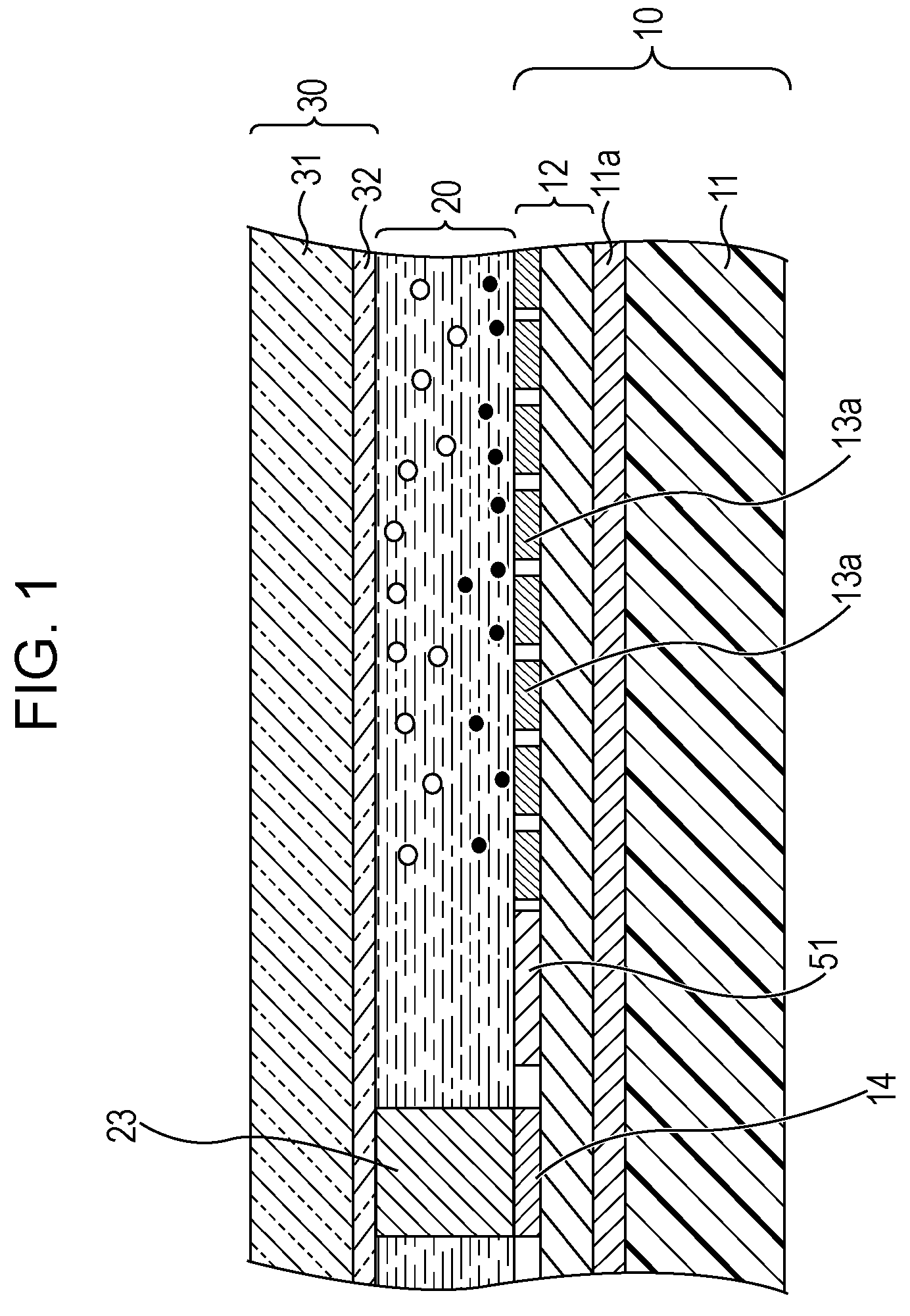
[0042]FIG. 1 is a diagram illustrating a section of an electrophoresis display device 1 which is an example of an electrophoresis device according to a first embodiment of the invention. As shown in the figure, the electrophoresis display device 1 roughly includes a first substrate 10, an electrophoresis layer 20, and a second substrate 30. In the figure, the surface close to the second substrate 30 serves as an observation surface and an image is observed through the second substrate 30.

[0043]In the first substrate 10, a thin-film semiconductor circuit layer 12 is formed on a flexible substrate 11 as an insulating base for forming an electrical circuit.

[0044]The flexible substrate 11 is, for example, a polycarbonate substrate having a thickness of about 200 μm. The thin-film transistor semiconductor circuit layer 12 is formed on (bonded to) the flexible substrate 11 with an adhesive layer 11a formed of, for example, a UV-curable adhesive therebetween. The flexible substrate 11 may ...

second embodiment

[0080]Although the pixel electrode 13a constituting a pixel is divided into two sub-pixel electrodes in the first embodiment, the pixel electrode 13a constituting a pixel may be divided into three or more sub-pixel electrodes. In this case, a transistor as a switching element is connected to each sub-pixel electrode. The gates of the transistors are connected to the corresponding scanning line Ym and the sources thereof are connected to the signal lines Xn-1, Xn-2, and Xn-3, respectively. With this configuration, by supplying a selection signal to a desired scanning line in the state where a proper voltage to the signal line, voltages can be individually applied to the sub-pixel electrodes through the selected switching element.

[0081]FIGS. 10A and 10B are diagrams illustrating a method of driving an electrophoresis display device 1 according to a second embodiment of the invention.

[0082]As shown in the figure, a pixel electrodes is divided into three sub-pixel electrodes 13a-1, 13a-...

third embodiment

[0092]FIGS. 11A to 11C are diagrams illustrating a method of driving an electrophoresis display device 1 according to a third embodiment of the invention.

[0093]As shown in the figures, in the third embodiment, a pixel electrode 13a is divided into a sub-pixel electrode 13a-1 and a sub-pixel electrode 13a-2 and a transparent electrode layer 32 is divided into a sub transparent electrode (third partial electrode) and a sub transparent electrode (fourth partial electrode) 32-2. Different voltages can be applied to the sub transparent electrode 32-1 and the sub transparent electrode 32-2, respectively.

[0094]First, in the state shown in FIG. 11A, the black particles are distributed close to the transparent electrode layer 32 as the observation surface and the black display is observed by an observer. A case where this state is changed to the white display will be described as an example.

[0095]First, as shown in FIG. 11B, the controller 52 applies potentials V1, V2, V3, and V4 to the sub-...


PUM


Abstract

An electrophoresis device is provided which includes: a display area including electrophoresis elements, each of which has a dispersion system, which includes first electrophoresis particles and second electrophoresis particles having different electrical polarities, between a first electrode and a second electrode disposed opposite to each other; and a voltage control unit allowing the first and second electrophoresis particles to migrate to the first and second electrodes, respectively, so as to form an image by applying a voltage to the electrophoresis elements. Here, the first electrode has a first partial electrode and a second partial electrode and the voltage control unit unevenly distributes the electrophoresis particles distributed close to the first electrode onto one of the first and second partial electrodes by applying different voltages to the first partial electrode and the second partial electrode prior to changing display.

Description

BACKGROUND[0001]1. Technical Field[0002]The present invention relates to an electrophoresis device, an electronic apparatus, and a method of driving the electrophoresis device.[0003]2. Related Art[0004]A known example of an electrophoresis display device is known which has a structure in which an electrophoresis dispersion liquid including a liquid dispersion medium and at least two types of electrophoresis particles is disposed between a pair of electrodes disposed opposite each other. Such an electrophoresis display device is disclosed in JP-A-62-269124.[0005]In the electrophoresis device having the above-mentioned structure, for example, positively charged white particles and negatively charged black particles are dispersed between the electrodes and two types of electrophoresis particles migrate to several electrodes in the direction of an electric field by applying a voltage across the electrodes. By dividing one electrode into a plurality of pixel electrodes and controlling th...

Claims


Application Information

Patent Timeline
IPC IPC(8): G09G3/34G02F1/167G02F1/1685
CPCG02F1/167G09G3/2074G09G2300/0809G09G2300/0443G09G3/3446G02F1/1685
Inventor KAWAI, HIDEYUKI
Owner SEIKO EPSON CORP
Why Eureka
Try Eureka