

Data management and control system in semiconductor flush memory and semiconductor flush memory accommodation apparatus
a data management and control system technology, applied in memory adressing/allocation/relocation, instruments, computing, etc., can solve the problems of irregular changes in increase the time required for synchronization processing, so as to reduce the delay of data read operation, extend the service life of semiconductor flush memory, and ensure the effect of synchronization processing
- Summary
- Abstract
- Description
- Claims
- Application Information
AI Technical Summary
Benefits of technology
Problems solved by technology
Method used
Image

Examples
first embodiment
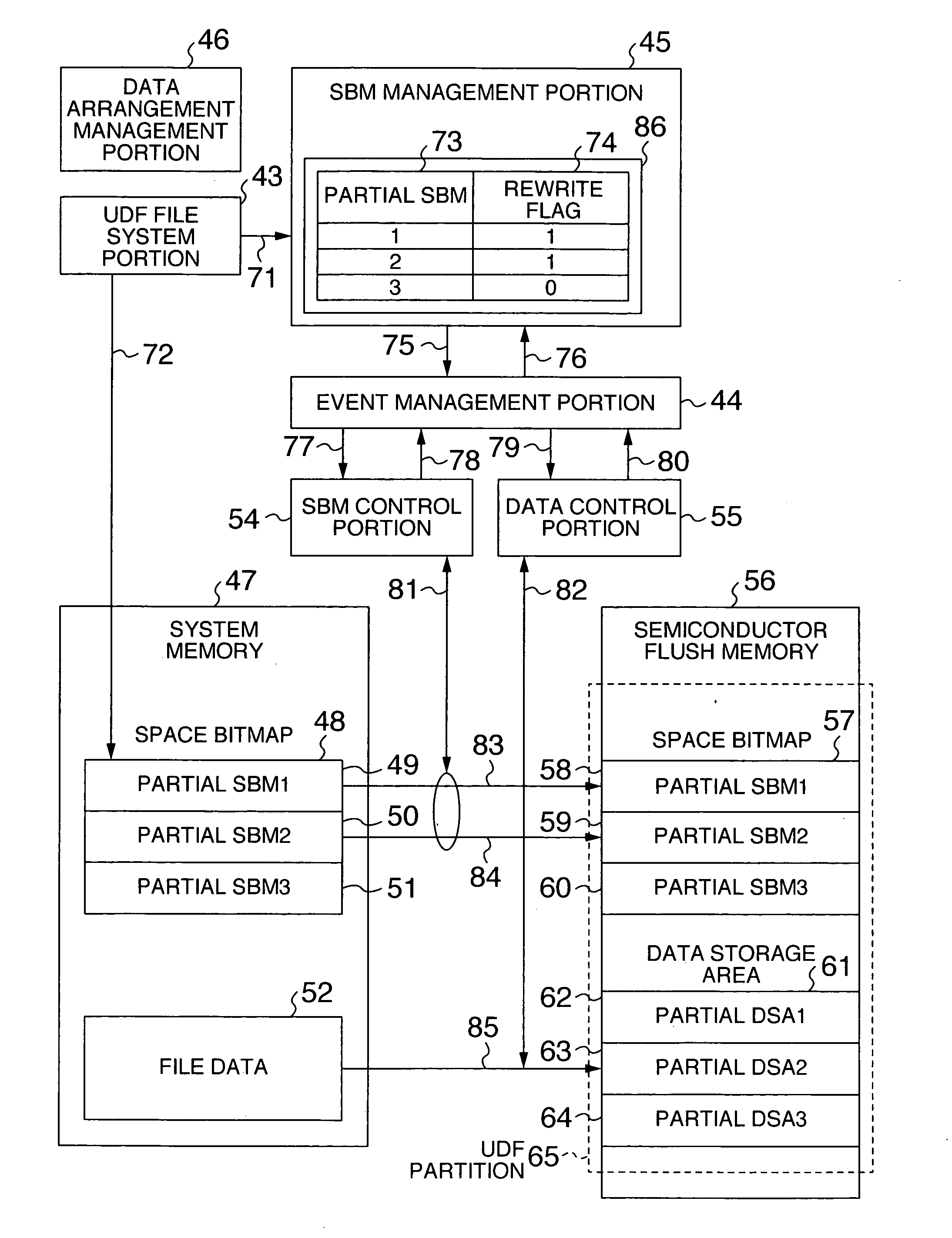
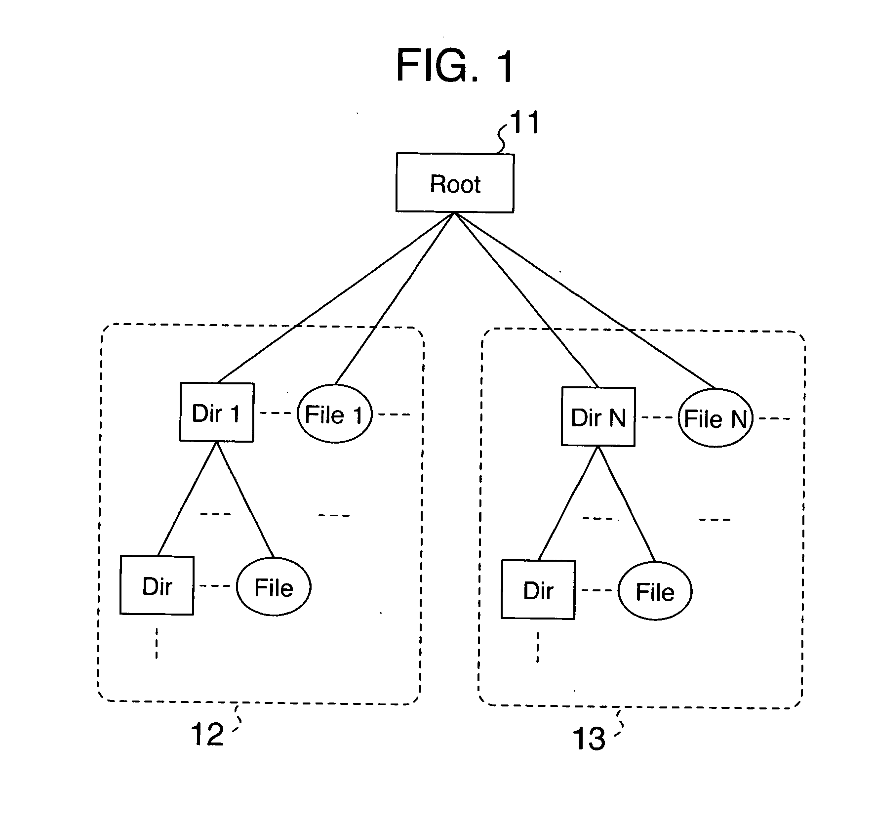
[0037]A semiconductor flush memory accommodation apparatus equipped with a data management and control system according to the first embodiment of the invention will be hereinafter explained with reference to FIGS. 1 and 4. FIG. 1 is a view showing a directory structure to which file data belongs, for explaining a mapping rule applied to the data management and control system according to the first embodiment of the invention. FIG. 4 is a block diagram showing a semiconductor flush memory accommodation apparatus equipped with the data management and control system according to the first embodiment of the invention.
[0038]Referring to FIG. 4, the semiconductor flush memory accommodation apparatus 41 includes data management means 42, data control means 53, a system memory 47 and a semiconductor flush memory 56. The semiconductor flush memory 56 is so constituted as to execute data erasure in a block unit. In the example shown in FIG. 4, as will be later explained, portions SBM1, SBM2 ...
second embodiment
[0080]A data management method and a control system according to the second embodiment of the invention will be explained with reference to FIGS. 8 and 9.
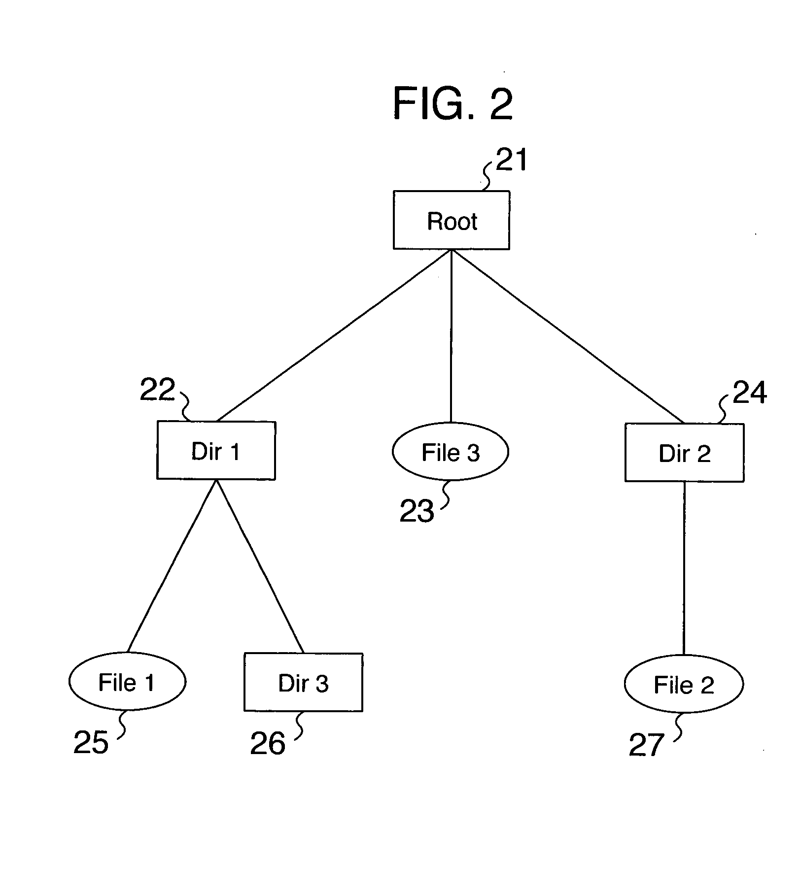
[0081]FIG. 8 shows the case where the space bitmap 57 in the semiconductor flush memory 56 shown in FIG. 4 is so arranged as to spread over three blocks. The drawing shows a directory structure to which the file data 52 on the system memory 47 recorded to the data storage area 61 of the semiconductor flush memory 56 belongs.
[0082]With reference to the semiconductor flush memory accommodation apparatus 41 shown in FIG. 4, the first file directory group 144 inclusive of the Root directory 141 is recorded to the partial DSA1 (62) corresponding to the partial SBM1 (58) shown in FIG. 4 in the second embodiment of the invention provided by the data arrangement management portion 46 of the data management means 42. The second directory group 145 arranged below the Root directory 141 and including a certain Dir1 (142) is recorded to the pa...
PUM
 Abstract
Description
Claims
Application Information