Display device including optical sensor in pixel

a display device and optical sensor technology, applied in static indicating devices, non-linear optics, instruments, etc., can solve the problems of inability to maintain white balance and uneven aperture ratio of respective sub-pixels, and achieve the effect of maintaining display performan

Inactive Publication Date: 2007-10-04
TOSHIBA MATSUSHITA DISPLAY TECH
View PDF6 Cites 23 Cited by
  • Summary
  • Abstract
  • Description
  • Claims
  • Application Information

AI Technical Summary

Benefits of technology

[0008]An object of the present invention is to adjust the amount of light passing through the respective sub-pixels in each pixel when an image is displayed on a display device, and thus to maintain display performance.
[0010]In the present invention, the optical sensor is disposed across the three sub-pixels in each of the pixel. This configuration makes it possible to adjust the aperture ratios of the respective sub-pixels, and thus to make the amount of light passing through the respective sub-pixels closer to one another, when an image is displayed.
[0012]In the present invention, the optical sensor is disposed in any one of the three sub-pixels in each of the pixel, and the dummy patterns are respectively disposed in the sub-pixels, in each of which the optical sensor is not disposed. This configuration makes it possible to adjust the aperture ratios of the respective sub-pixels, and thus to make the amount of light passing through the respective sub-pixels close to one another, when an image is displayed.

Problems solved by technology

Accordingly, aperture ratios of the respective sub-pixels are not uniform.
This results in a problem that white balance cannot be maintained.

Method used


Image

  • Display device including optical sensor in pixel
  • Display device including optical sensor in pixel
  • Display device including optical sensor in pixel

Examples


first embodiment

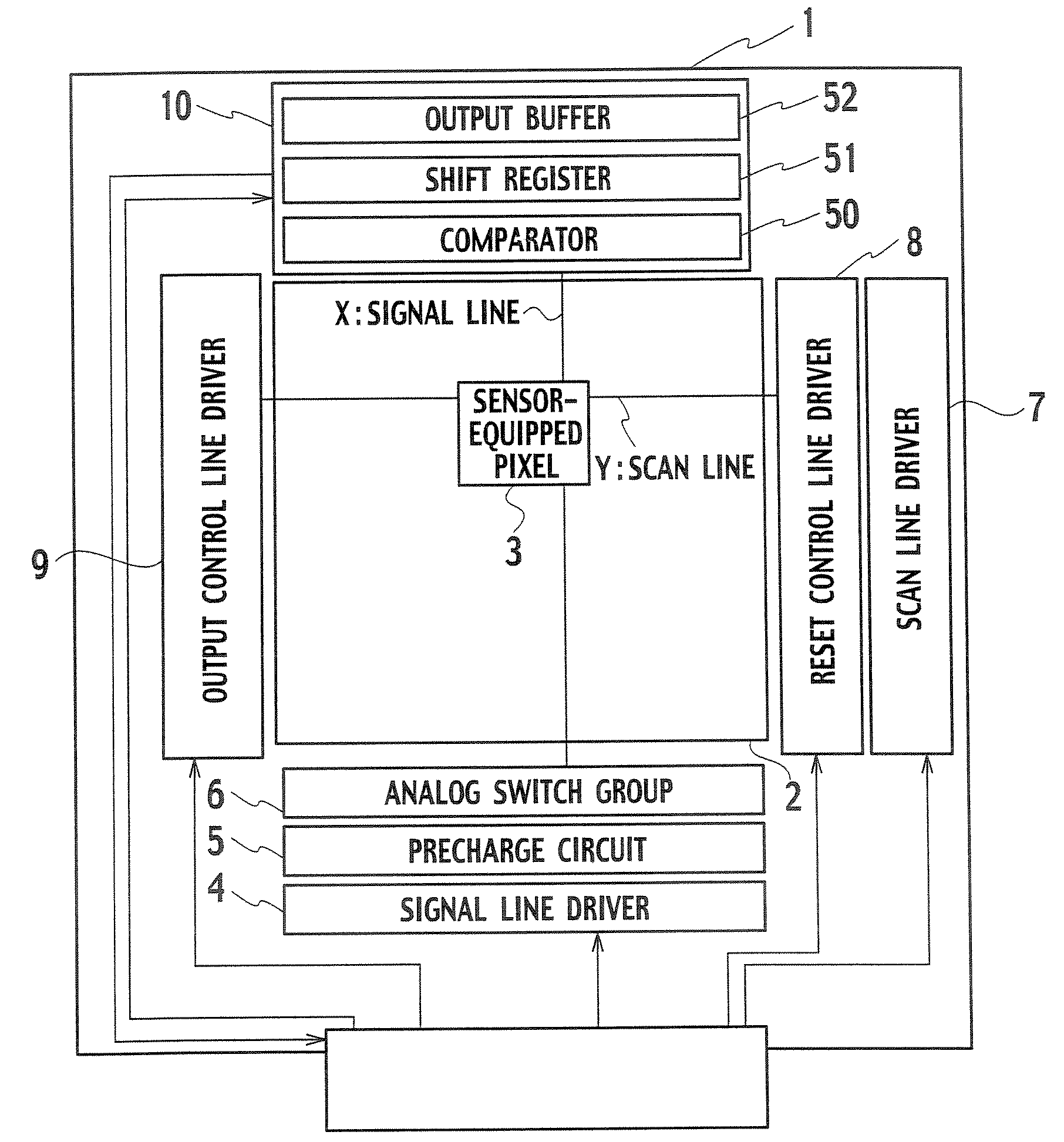
[0022]As shown in a block diagram of FIG. 1, the display device of this embodiment includes a pixel region 2 having a plurality of pixels and circuit regions entirely surrounding the pixel region 2 on a glass substrate 1.

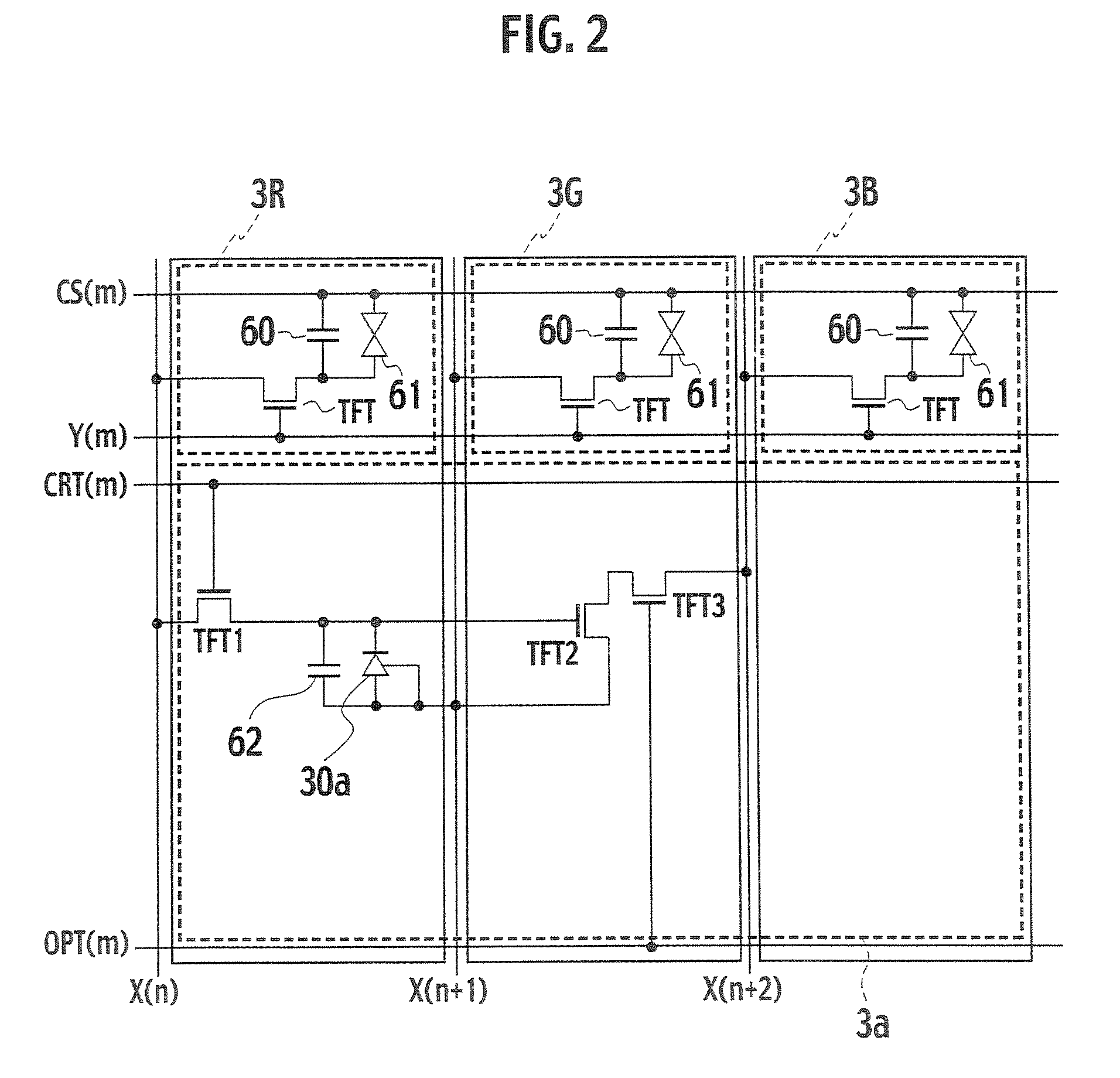
[0023]In the pixel region 2, scan lines Y and signal lines X are disposed intersecting each other. At each of the intersections, a pixel 3 including an optical sensor is disposed. Here, an XGA-type liquid crystal display panel is adopted as an example of the display device. In the pixel region 2, 768 scan lines and 3,072 signal lines are disposed intersecting each other.

[0024]In the circuit region below the pixel region 2, a signal line driver 4, a precharge circuit 5, and an analog switch group 6 are disposed. The signal line driver 4 supplies an image signal to each of the signal lines X. The precharge circuit 5 supplies a precharge voltage to each of the signal lines X. The analog switch group 6 consists of a plurality of analog switches each switching the connec...

second embodiment

[0042]A basic configuration of a display device of a second embodiment is similar to that described in the first embodiment. The second embodiment is different from the first embodiment in that dummy patterns are disposed in sub-pixels in each of which no optical sensor is disposed.

[0043]As shown in a layout diagram of a pixel of FIG. 6, an optical sensor 3b is disposed in a green sub-pixel 3G. Dummy patterns 12 are respectively disposed in sub-pixels 3R and 3B, in each of which the optical sensor 3b is not disposed. The dummy pattern 12 has a function of blocking external light such as backlight when an image is displayed. This configuration makes it possible to adjust the aperture ratios of the respective sub-pixels, and thus to make the amount of light passing through the respective sub-pixels closer to one another.

[0044]As describe above, in the second embodiment, the optical sensor 3b is disposed in the green sub-pixel 3G, and the dummy patterns 12 are respectively disposed in ...

third embodiment

[0046]A basic configuration of a display device of a third embodiment is similar to that described in the first embodiment. The third embodiment is different from the first embodiment in that an optical sensor is disposed in a sub-pixel of three sub-pixels, the sub-pixel having an area larger than the other two pixels.

[0047]As shown in a layout diagram of a pixel of FIG. 7, an optical sensor 3c is disposed in a sub-pixel 3G of three sub-pixels 3R, 3G and 3B in a pixel 3. The sub-pixel 3G has an area larger than the other sub-pixels 3R and 3B. Here, a ratio of pixel pitches of the sub-pixels 3R, 3G and 3B is 46:63.5:43.5. The green sub-pixel 3G has the area larger than the sub-pixels 3R and 3B. This configuration makes it possible to make the amount of light passing through the respective sub-pixels closer to one another when an image is displayed.

[0048]As described above, in the third embodiment, the optical sensor 3c is disposed in the green sub-pixel 3G of the three sub-pixels 3R,...


PUM


Abstract

In order to maintain display performance of a display device, the display device includes an optical sensor disposed across three sub-pixels of red, green and blue colors in each pixel. This configuration makes it possible to adjust the aperture ratios of the respective sub-pixels, and thus to make the amount of light passing through the respective sub-pixels closer to one another. In other words, the white balance can be maintained.

Description

CROSS-REFERENCE TO RELATED APPLICATIONS[0001]This application is based upon and claims the benefit of priority from Japanese Patent Application No. 2006-95370 filed on Mar. 30, 2006; the entire contents of which are incorporated herein by reference.BACKGROUND OF THE INVENTION[0002]1. Field of the Invention[0003]The present invention relates to a display device having a function of reading light entering from a screen by using a sensor included in each pixel.[0004]2. Description of the Related Art[0005]Display devices, such as the display device described in Japanese Patent Application Laid-Open Official Gazette No. 2004-93894, have been developed in recent years. Such a display device includes not only pixels each located at an intersection of a scan line and a signal line, but also optical sensors in the respective pixels. The optical sensors detect the fact that a finger of a user comes close to, for example, a touch panel.[0006]In a display device of the prior art, each pixel inc...

Claims


Application Information

Patent Timeline
Patent Type & Authority Applications(United States)
IPC IPC(8): G09G3/36
CPCG02F1/1343G02F2001/13312G02F1/1362G02F1/13312
Inventor HAYASHI, HIROTAKAYAMADA, YOSHITAKANAKAMURA, TAKASHITADA, NORIONAKAMURA, HIROKI
Owner TOSHIBA MATSUSHITA DISPLAY TECH
Why Eureka
Try Eureka