Display panel and preparation method thereof

A display panel and substrate technology, which is applied in semiconductor/solid-state device manufacturing, electrical components, electric solid-state devices, etc., can solve the problems affecting the display effect of the display panel, the increase of resistance-capacitance circuit voltage, gate etching, etc. Show the effect of the effect

Active Publication Date: 2020-02-21
WUHAN CHINA STAR OPTOELECTRONICS SEMICON DISPLAY TECH CO LTD
View PDF5 Cites 2 Cited by
  • Summary
  • Abstract
  • Description
  • Claims
  • Application Information

AI Technical Summary

Problems solved by technology

[0003] In the existing display panel structure, due to the use of buffered oxide etchant (BOE) or hydrofluoric acid (HF) solution to clean the surface of the contact hole semiconductor, the source and drain (SD) and the semiconductor form a better Contact, but this will cause the gate to be severely etched at the same time, resulting in an increase in the co

Method used


Image

  • Display panel and preparation method thereof
  • Display panel and preparation method thereof
  • Display panel and preparation method thereof

Examples


Embodiment Construction

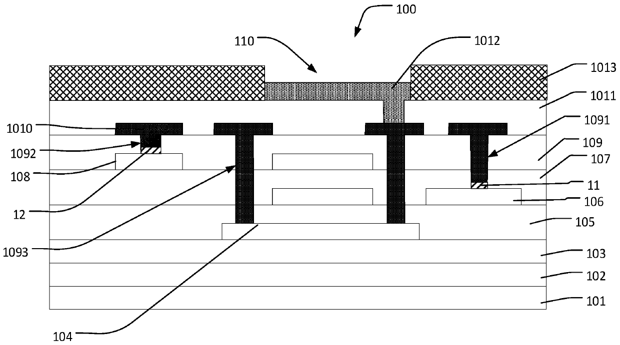
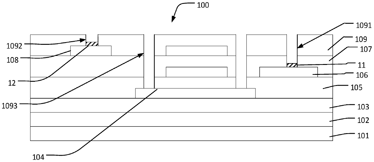
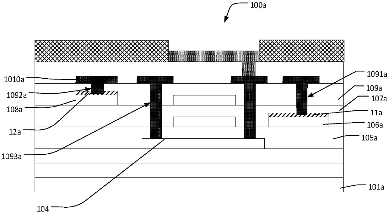
[0031] The following description of each embodiment refers to the attached drawings to illustrate specific embodiments in which the present invention can be implemented. The terms of direction mentioned in the present invention, such as up, down, front, back, left, right, inside, outside, side, etc., are only directions with reference to the drawings. The component names mentioned in the present invention, such as first, second, etc., only distinguish different components and can be better expressed. In the figures, units with similar structures are indicated by the same reference numerals.

[0032] The embodiments of the present invention will be described in detail herein with reference to the accompanying drawings. The present invention can be manifested in many different forms, and the present invention should not only be interpreted as the specific embodiments set forth herein. The present invention provides these embodiments to explain the practical application of the pre...


PUM


Abstract

The invention provides a display panel and a preparation method thereof. Oxide layers are arranged at the joints of a source-drain metal layer and a first gate layer and a second gate layer, specifically, a first oxide layer is arranged at a position, corresponding to a first through hole, of the first gate layer, and a second oxide layer is arranged at a position, corresponding to a second through hole, of the second gate layer. Or, oxide layers can be arranged on the whole surfaces of the first gate layer and the second gate layer. The first oxide layer and the second oxide layer are used for protecting the joint of the source-drain metal layer and the first gate layer or the second gate layer from being corroded by HF, so that the contact resistance of the source-drain metal layer and the first gate layer or the second gate layer is not affected, and the display effect of the display panel is kept stable.

Description

Technical field [0001] The invention relates to the field of display, in particular to a display panel and a preparation method thereof. Background technique [0002] Organic Light-Emitting Diode (OLED), due to its light weight, self-luminous, wide viewing angle, low driving voltage, high luminous efficiency, low power consumption, and fast response speed, has become more and more widely used, especially flexible The OLED display device has the characteristics of being bendable and easy to carry, and has become the main field of research and development in the field of display technology. [0003] In the existing display panel structure, because the buffer oxide etching solution (BOE) or hydrofluoric acid (HF) solution is used to clean the surface of the contact hole semiconductor, the source and drain (SD) and the semiconductor are formed well. Contact, but this will also cause the gate to be severely etched, resulting in an increase in the contact resistance between the source a...

Claims


Application Information

Patent Timeline
IPC IPC(8): H01L27/32H01L21/77
CPCH10K59/1213H10K59/131H10K59/1201
Inventor 杨薇薇
Owner WUHAN CHINA STAR OPTOELECTRONICS SEMICON DISPLAY TECH CO LTD
Why Eureka
Try Eureka