Far-field optical microscope with a nanometer-scale resolution based on the in-plane image magnification by surface plasmon polaritions

a far-field optical microscope and in-plane image technology, applied in the field of optical microscopy, can solve the problems of limited resolution of regular optical microscopes, limited range of refractive indexes of immersion microscopes, and inability to use microscopes as versatile and convenient as regular far-field optical microscopes. achieve the effect of improving resolution and optical resolution

Inactive Publication Date: 2007-10-04
UNIV OF MARYLAND
View PDF1 Cites 6 Cited by
  • Summary
  • Abstract
  • Description
  • Claims
  • Application Information

AI Technical Summary

Benefits of technology

[0010] The present disclosure describes a far-field optical microscope capable of reaching nanometer-scale resolution using the in-plane image magnification by surface plasmon polaritons, also known as two-dimensional light, which is made of electromagnetic waves coupled with conducting electrons. The immersion microscope of the present disclosure improves resolution using an approach based on the optical properties of a metal-dielectric interface that may provide extremely large values of the effective refractive index neff up to 103 as seen by surface polaritons. Thus, the diffraction limited resolution can reach nanometer-scale values of λ / 2neff. The experimental realization of such an immersion microscope has demonstrated the optical resolution better than 50 nm at 502 nm illumination wavelength.
[0011] The microscopy technique employed by the immersion microscope of the present disclosure improves resolution without expensive equipment and special preparations needed for electron microscopes and other technologies. The microscopy technique entails coaxing plasmon polaritons into magnifying images by placing a microscopic sample onto a thin, coated glass surface (such as a meta-coated glass surface that supports propagation of surface electromagnetic waves), like a document on the surface of a photocopier, and depositing a drop of glycerin or other substance on top of it. Alternatively, instead of depositing a drop of glycerin or other substance, a solid parabolically shaped dielectric layer can be provided on the metal surface. Laser light is then propagated or shined through the glass creating surface plasmon polaritons in the metal-coating. The plasmon polaritons “sense” the sample by scattering off of it. They can sense finer details than ordinary light because their wavelength is only 70 nm, seven times shorter than that of the laser.

Problems solved by technology

Unfortunately, the resolution of a regular optical microscope is limited by the wavelength of visible light.
Immersion microscopes introduced by Ernst Abbe in the 19th century have slightly improved resolution on the order of λ / 2n because of the shorter wavelength of light λ / n in a medium with refractive index n. However, immersion microscopes are limited by the small range of refractive indices n of available transparent materials.
Although many fascinating results are obtained with near-field optics, such microscopes are not as versatile and convenient to use as regular far-field optical microscopes.

Method used


Image

  • Far-field optical microscope with a nanometer-scale resolution based on the in-plane image magnification by surface plasmon polaritions
  • Far-field optical microscope with a nanometer-scale resolution based on the in-plane image magnification by surface plasmon polaritions
  • Far-field optical microscope with a nanometer-scale resolution based on the in-plane image magnification by surface plasmon polaritions

Examples


Embodiment Construction

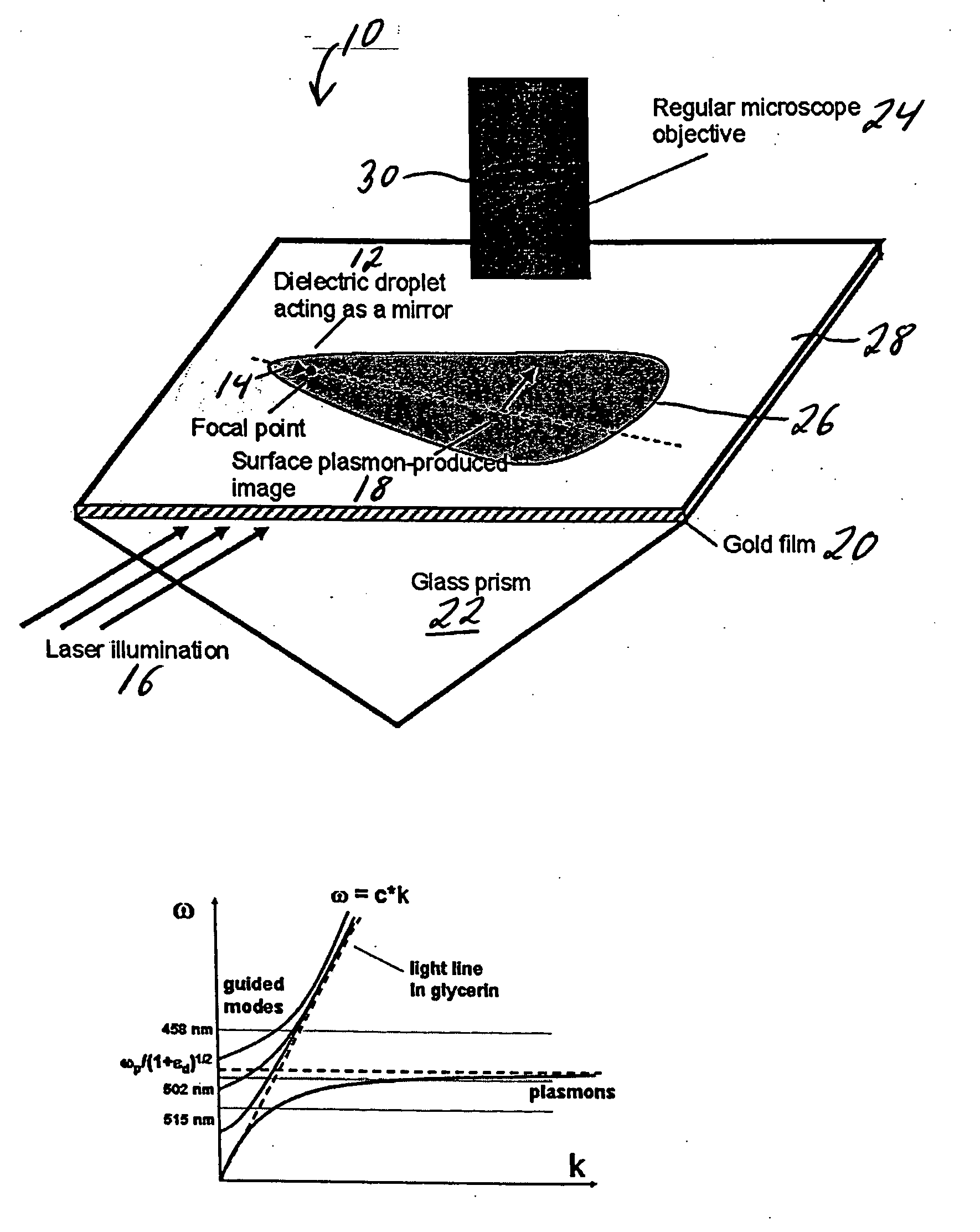
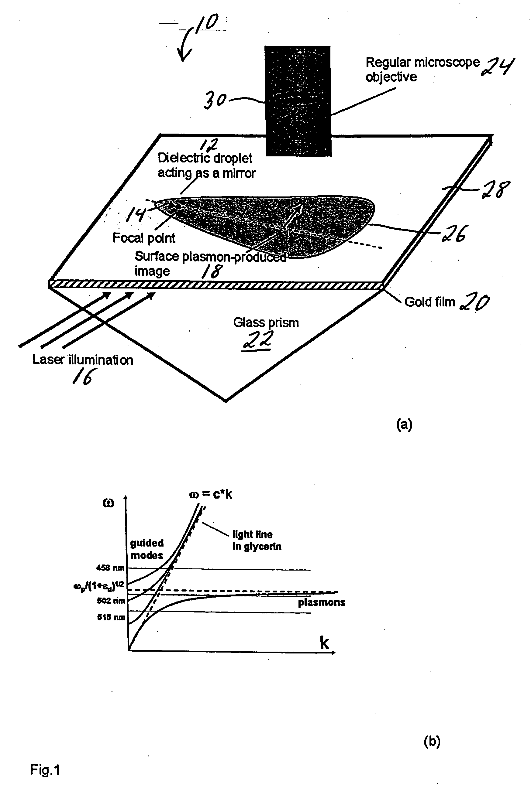
[0032] The present disclosure describes a far-field optical microscope capable of reaching nanometer-scale resolution using the in-plane image magnification by surface plasmon polaritons based on the optical properties of a metal-dielectric interface that may provide extremely large values of the effective refractive index neff up to 103 as seen by surface polaritons, and thus the diffraction limited resolution can reach nanometer-scale values.

I. Introduction

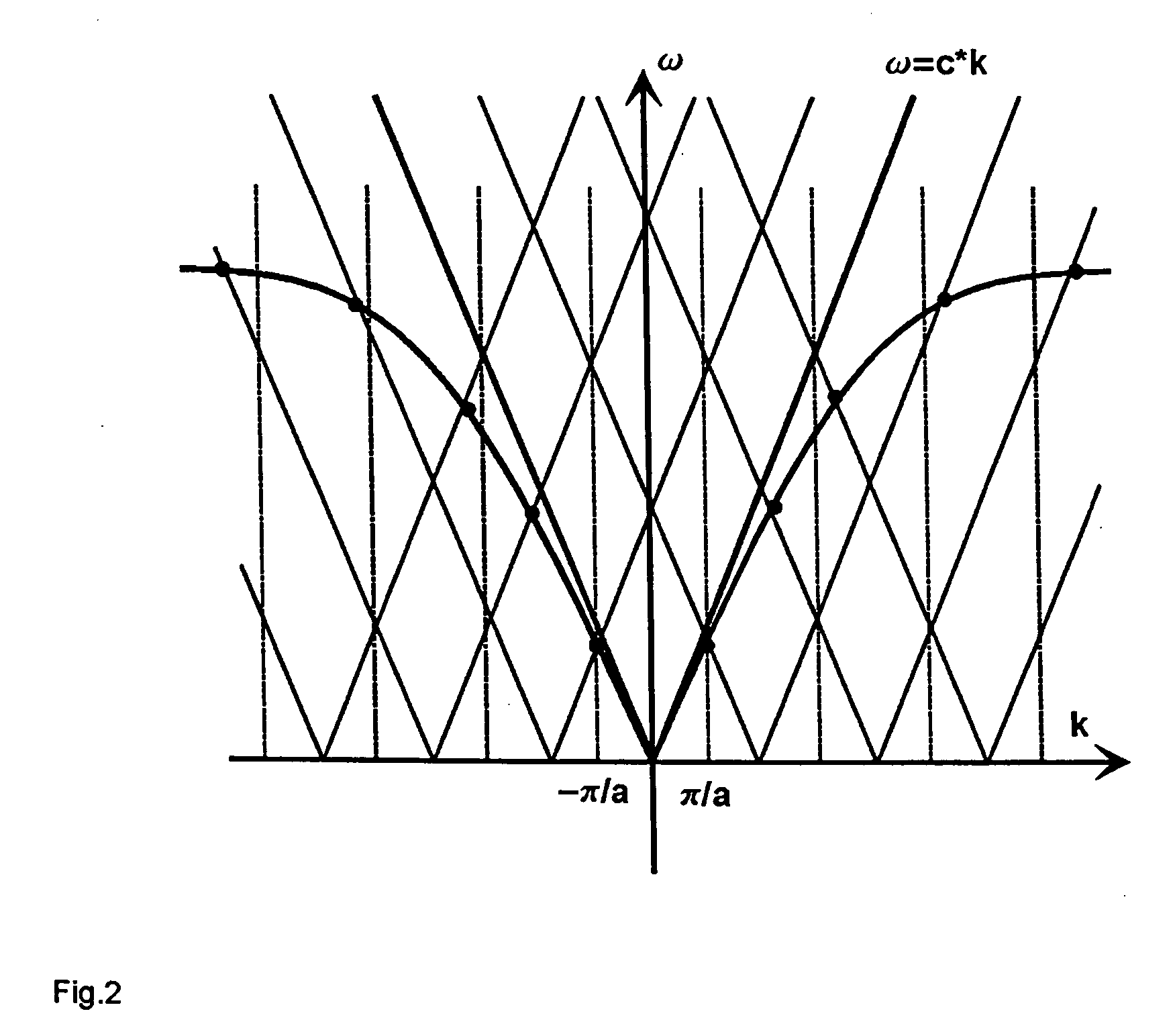
[0033] The wave vector of a surface plasmon propagating over an interface between a dielectric and an infinitely thick metal film is defined by the expression kp=ωc⁢(ɛd⁢ɛmɛd+ɛm)1 / 2(1)

where εm(ω) and εd(ω) are the frequency-dependent dielectric constants of the metal and dielectric, respectively. If the imaginary part of the metal's dielectric constant is neglected, under the resonant condition

εm(ω)=−εd(ω)   (2)

both phase and group velocities of the surface plasmons tend to zero. This means that the wavelength λp of such ...


PUM

PropertyMeasurementUnit
wavelengthaaaaaaaaaa
thickaaaaaaaaaa
wavelengthaaaaaaaaaa

Abstract

A far-field optical microscope capable of reaching nanometer-scale resolution using the in-plane image magnification by surface plasmon polaritons is presented. The microscope utilizes a microscopy technique based on the optical properties of a metal-dielectric interface that may, in principle, provide extremely large values of the effective refractive index neff up to 102-103 as seen by the surface plasmons. Thus, the theoretical diffraction limit on resolution becomes λ / 2neff, and falls into the nanometer-scale range. The experimental realization of the microscope has demonstrated the optical resolution better than 50 nm for 502 nm illumination wavelength.

Description

PRIORITY [0001] This application is a continuation application of an application filed on Feb. 18, 2005 and assigned U.S. application Ser. No. 11 / 061,837 which claims priority under 35 U.S.C. §119(e) to a United States Provisional Application filed on Feb. 20, 2004 and assigned U.S. Provisional Application No. 60 / 546,146 and to a United States Provisional Application filed on May 7, 2004 and assigned U.S. Provisional Application No. 60 / 569,305. The contents of all priority applications are incorporated herein by reference.STATEMENT REGARDING FEDERALLY SPONSORED RESEARCH [0002] This invention was made with government support under NSF contract nos. ECS-0210438 and ECS-0304046 awarded by the National Science Foundation. The government has certain rights in this invention.BACKGROUND OF THE INVENTION [0003] 1. Technical Field [0004] The disclosure relates to optical microscopy. In particular, the disclosure relates to a far-field optical microscope with a nanometer-scale resolution base...

Claims


Application Information

Patent Timeline
Patent Type & Authority Applications(United States)
IPC IPC(8): G01N21/55G01N21/01
CPCG01N21/01G01N2021/178G01N21/554
Inventor SMOLYANINOV, IGOR I.DAVIS, CHRISTOPHER C.
Owner UNIV OF MARYLAND
Why Eureka
Try Eureka