Method and System for Context-Specific Mask Inspection

a mask and context-specific technology, applied in the field of masks, can solve the problems of extreme precision for sub wavelengths, the resolution limit of optical lithography technology is increasingly being challenged, and the overall polygonal figure count is skyrocketing

Inactive Publication Date: 2007-10-04
CADENCE DESIGN SYST INC
View PDF60 Cites 36 Cited by
  • Summary
  • Abstract
  • Description
  • Claims
  • Application Information

AI Technical Summary

Problems solved by technology

The resolution limit of today's optical lithography technology is increasingly being challenged by the sub wavelength, or low-k1, dimensions of the critical IC feature geometries.
Furthermore, due to the necessity to mitigate optical proximity effect distortions through resolution enhancement techniques at the mask level, the overall polygonal figure count is skyrocketing.
Extreme precision is required for sub wavelength (or low-k1) applications, due to highly non-linear imaging behaviors which often magnify mask errors by large factors.
The overall design and manufacturing process integration complexity is also expanding, as it attempts to span a widening and deepening gap between the different technical disciplines and ‘cultures’ of manufacturing and design.
This has led to increases in the length of time to create and inspect masks, in the number of errors impacting mask elements, and in the costs associated with the mask process.
However, a wealth of design knowledge is stripped out of this geometry-only format, and therefore is unavailable to any data file derived from it or any design or manufacturing integration process performed thereafter.
Due to fundamental inherent limitations in current and near-future optical lithography processes, the layout of the IC design is no longer directly equivalent to the pattern printed on the eventual IC wafer.
However, like the GDS-II stream file, this file holds none of the higher-level IC design, circuit feature functionality, or criticality information available in the IC design flow.
However, there is no ‘knowledge’ of what a feature is beyond its geometry and location.
There is a tradeoff between optimizing writing speed and the deleterious effects of thermal, chemical and proximity effects related to the writing speed.
The design data connectivity and ‘design intent’ have been destroyed by this point.
As the IC industry moves to deep sub-wavelength, or ‘low-k1’ layout features, lens aberrations may increasingly violate these space-invariance assumptions, requiring additional higher-level consideration in the design flow as well as the mask flow.
However, the time demands of the latter can be enormous, resulting in inspection equipment utilizing and requiring increasingly computationally powerful parallel computer architectures.
Aside from cosmetic defects, defects in a mask are generally assumed to result in defects in an integrated circuit replicated from that mask.
The process of classifying and waiving defects on this basis may be performed by a time consuming manual technique.
Additionally, when an unintended artifact is found, there may be no means for interpreting whether this artifact is a defect in the context of its impact on the circuit feature and manufacturing goals.
Typically, deviations from the ideal design are considered defects.
Defects may also include opaque or transparent errors on a mask.
Such transparent defects may impact the phase of light passing through them resulting in unwanted optical interference effects, while opaque defects block or alter such light in some way.
However, mask repair 114 performed by ion beam milling or other repair processes, may be more time-consuming and expensive than writing a new mask.
Additionally, mask repair often creates further defects in a mask, by adding unwanted material during the ion milling process.
The repair process may also erode the mask elements in an unwanted manner.
Merely handling the mask may alter or damage it through any number of means, including electrostatic discharge (ESD).
This repetitive cycle of inspecting, repairing, and inspecting again is often costly and time-consuming.

Method used


Image

  • Method and System for Context-Specific Mask Inspection
  • Method and System for Context-Specific Mask Inspection
  • Method and System for Context-Specific Mask Inspection

Examples


Embodiment Construction

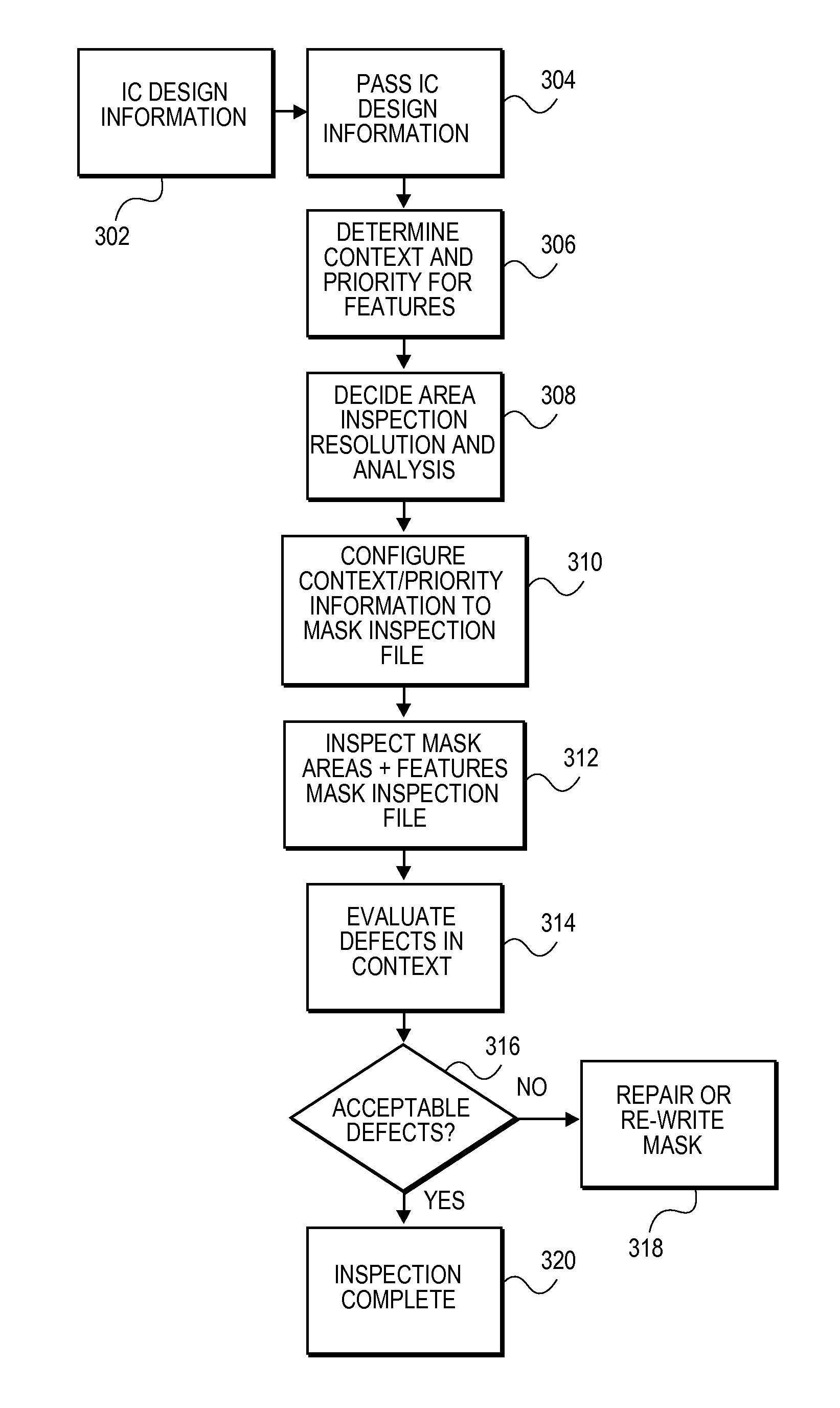
[0031] A method and system is provided for improving mask inspection processes. In an embodiment, the information developed in designing an integrated circuit and photomask are used to give context to polygonal shapes that are inspected on a mask. Polygonal shapes of various circuit elements are inspected in light of their associated contextual information, such as priority, ordering, or inspection parameter information, for example. The contextual information may be added to a database and emphasized for use in guiding the mask inspection process. The contextual information may also include both manufacturing and circuit context parameters, and be used in processes that prioritize and order various features of the circuit or mask designs.

[0032] Contextual information related to the manufacturing process may include, for example: specified resolution; criticality; proximity-effect distortions; topological properties of a circuit layer resulting from mask features; chemical or therm...


PUM

PropertyMeasurementUnit
electricalaaaaaaaaaa
poweraaaaaaaaaa
electrical intentaaaaaaaaaa

Abstract

A method for inspecting lithography masks includes generating integrated circuit design data and using context information from the integrated circuit design data to inspect a mask.

Description

CROSS REFERENCE TO RELATED APPLICATIONS [0001] This application is a divisional of U.S. patent application Ser. No. 10 / 620,284, filed on Jul. 14, 2003, which claims the benefit of U.S. Provisional Application No. 60 / 395,467, filed Jul. 12, 2002, both of which are incorporated herein by reference in their entirety.FIELD OF THE INVENTION [0002] The present invention relates to the field of photomasks for photolithographic production of integrated chips. BACKGROUND OF THE INVENTION [0003] Photolithography is a fabrication process by which patterns for various devices, such as integrated circuits (IC), are generated on substrate wafers. This process generally starts with the design of an IC chip, including the various circuit elements, their electrical interconnects, and their physical layout across the chip. The IC design typically describes each layer required to fabricate the IC in a FAB using a photolithographic process. There are generally many layers to an IC chip. [0004] After an...

Claims


Application Information

Patent Timeline
Patent Type & Authority Applications(United States)
IPC IPC(8): G06F19/00G03FG03F1/84G03F9/00G06F7/60G06F17/10
CPCG03F1/84
Inventor PACK, ROBERT C.SCHEFFER, LOUIS K.
Owner CADENCE DESIGN SYST INC
Why Eureka
Try Eureka