Electrical mask inspection

a technology of mask inspection and electric field, applied in the direction of individual semiconductor device testing, semiconductor/solid-state device testing/measurement, instruments, etc., can solve the problems of reduced die yield, substantial yield loss, and defect that can occur with repeated use of the photo mask

Inactive Publication Date: 2012-03-22
IBM CORP
View PDF19 Cites 12 Cited by
  • Summary
  • Abstract
  • Description
  • Claims
  • Application Information

AI Technical Summary

Benefits of technology

[0006]Another embodiment of the present invention provides a method for testing an integrated circuit. The method comprises the steps of: forming a plurality of scan chains, each scan chain formed by the steps of: forming a first endpoint; forming a second endpoint; forming a first metal layer, comprising a plurality of segments; forming a second metal layer, comprising a plurality of segments; forming a via layer, comprising a plurality of vias wherein each via is configured and disposed to connect a segment of the first metal layer to a

Problems solved by technology

Printable defects on photomasks and reticles have historically been a source of defects that have reduced die yields.
When defects are p

Method used


Image

  • Electrical mask inspection
  • Electrical mask inspection
  • Electrical mask inspection

Examples


Embodiment Construction

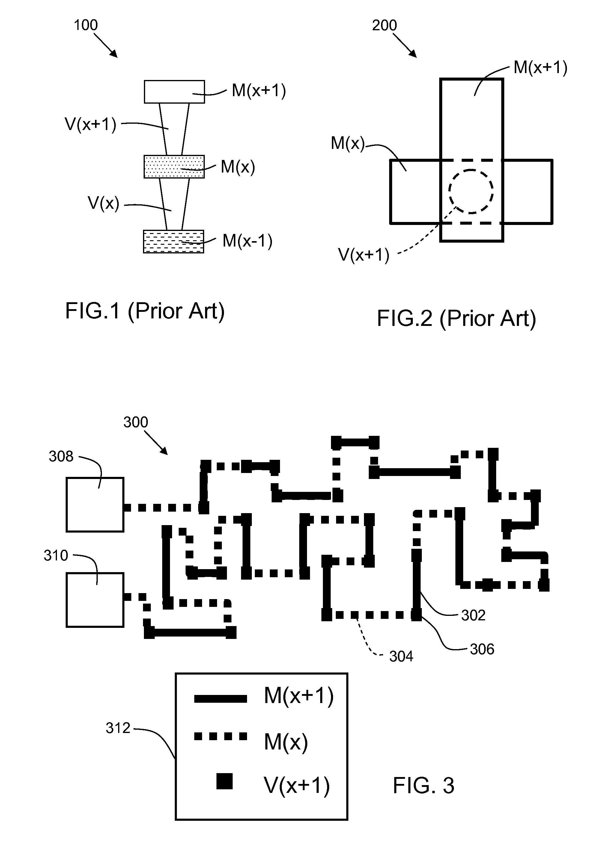
[0017]FIG. 1 is a side view of a portion of a multiple layer integrated circuit 100. At certain points within the integrated circuit, two metal layers are electrically connected by conductive vias. As shown in FIG. 1, metal layer M(x) is connected to metal layer M(x−1) with a via at via layer V(x). Furthermore, metal layer M(x) is connected to metal layer M(x+1) with via level V(x+1).

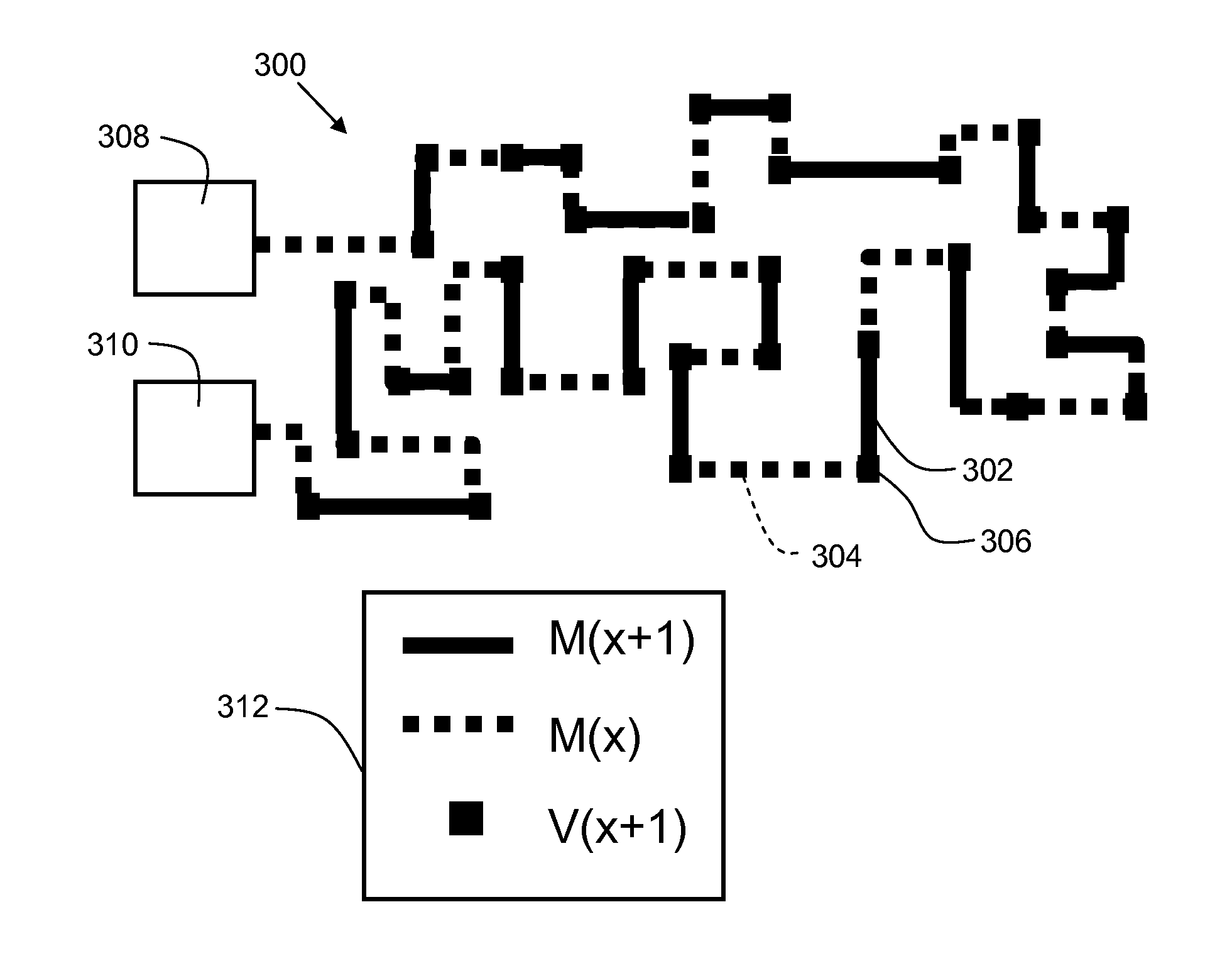
[0018]FIG. 2 is a top view of a portion of a multiple layer integrated circuit 200. Metal layer M(x+1) is electrically connected to metal layer M(x) through via layer V(x+1). In general, an integrated circuit may be comprised of millions of devices, such as transistors and capacitors interconnected by multiple metal layers and via layers. Testing connectivity at each “level” (e.g. M1, M2, V1, etc. . . . ) of an integrated circuit can be challenging. Embodiments of the present invention serve to provide an effective way to periodically check the masks corresponding to various levels. A functional level i...


PUM


Abstract

An apparatus and method for electrical mask inspection is disclosed. A scan chain is formed amongst two metal layers and a via layer. One of the three layers is a functional layer under test, and the other two layers are test layers. A resistance measurement of the scan chain is used to determine if a potential defect exists within one of the vias or metal segments comprising the scan chain.

Description

FIELD OF THE INVENTION[0001]The present invention relates generally to semiconductor fabrication, and more specifically to techniques for inspecting and verifying masks used in the fabrication of semiconductors.BACKGROUND OF THE INVENTION[0002]The capacity of integrated circuits has increased primarily as the result of reductions in the size of features on a semiconductor chip. The lateral dimensions of features are generally defined by photolithographic techniques in which a detailed pattern is transferred to a reactive material by shining light through a photomask or reticle. In this disclosure, the term “photomask” is interchangeable with the term “reticle.” During the photolithography process, energy is applied to photoresist deposited on a wafer, where the energy application is controlled through the use of a patterned photomask. The exposure to the wafer is made by a step and repeat procedure. In this procedure, the wafer is moved and the steppers are used to move and repeat t...

Claims


Application Information

Patent Timeline
IPC IPC(8): H01L23/522H01L21/66H01L21/768
CPCH01L23/544H01L22/34H01L2924/0002H01L2924/00
Inventor KUMAR, ARVINDCHOU, ANTHONY I-CHIHNARASIMHA, SHREESH
Owner IBM CORP
Why Eureka
Try Eureka