Mask defect analysis system

a mask and defect technology, applied in the field of mask defect analysis system, can solve the problems of mask rejection, chip failure, non-discrimination of approach, etc., and achieve the effects of saving cost and time of repair, preventing defects, and speeding up the measurement process

Inactive Publication Date: 2007-08-14
IBM CORP
View PDF23 Cites 13 Cited by
  • Summary
  • Abstract
  • Description
  • Claims
  • Application Information

AI Technical Summary

Benefits of technology

[0011]In another aspect of the present invention, the method can be applied to both the inspection and the pre-acceptance process. During either process, masks that have defects can be accepted, rather than repaired, if the defects are within acceptable deviations from the design tolerances. This allows the repair process to be skipped altogether if it is determined that the defects so identified will not cause product failure (e.g., defects in non-critical areas of the mask, or defects are within acceptable tolerances). By eliminating unnecessary repairs, the cost and time of repair are saved. Furthermore, this can prevent the defects that are sometimes generated (or exacerbated) by the repair process itself.
[0012]In another aspect of the present invention, the system uses a set of heuristic rules for determining whether a given mask defect will be resolved on the wafer by the photolithographic process. Alternatively, that determination can be made using one of a variety of commercially available tools such as NumeriTech's Virtual Stepper â,,℄ or the output of the AIMS tool. Heuristic rules for whether or not a defect would be resolved on the wafer would include defect size limits and limits on the defect placement relative to shapes from the design layout data. These rules are developed by empirical data on printed defects as well as photolithographically modeled results. Output from commercially available software (NumeriTech's Virtual Stepper â,,℄ or the aerial image data from the AIMS tool) provides a more reliable method of determining whether or not a defect would be resolved on the wafer by modeling the photolithographic pattern transfer process. Ultimately, those mask defects which are resolved on the wafer would then be analyzed to determine if they were problematic.
[0013]In another aspect of the present invention, a mask is inspected for defects in order to evaluate the effect of defects. Defect locations are analyzed to classify the defects into critical defects and non-critical defects. The final disposition of the mask is determined by applying different acceptance rules to the critical defects and the non-critical defects. A standard acceptance rule is applied to the defects located in the critical portions of the mask while a loose acceptance rule is applied to the defects located outside of the critical portions. When the loose acceptance rule is applied, the non-critical defects are considered as the candidates for a looser mask acceptance criteria. The critical dimension measurement is selectively performed only to the critical defects and routed to a repair step 240 or a scrapping step 250. Thus, according to the present invention, the time consuming critical dimension measurements are performed restrictedly to the critical portions, thereby speeding up the measurement process.

Problems solved by technology

In any event, the standard inspection process will tend to result in the rejection of masks when the size of the defect exceeds some maximum pre-established criterion.
This approach is non-discriminating, however, because it is well known that not all defects in a given mask will necessarily lead to failure of the chip.
Accordingly, the standard approach can lead to the rejection of masks with defects in non-critical regions of the chip layout.
Based on this standard approach, otherwise acceptable masks would be scrapped unnecessarily.
However, in general, such techniques cannot resolve issues involving nets because simple inspection of the mask or the layout data does not suffice to accurately define the nets.
In any event, either option is labor intensive and expensive and can be detrimental to the manufacturing process.

Method used


Image

  • Mask defect analysis system
  • Mask defect analysis system
  • Mask defect analysis system

Examples


Embodiment Construction

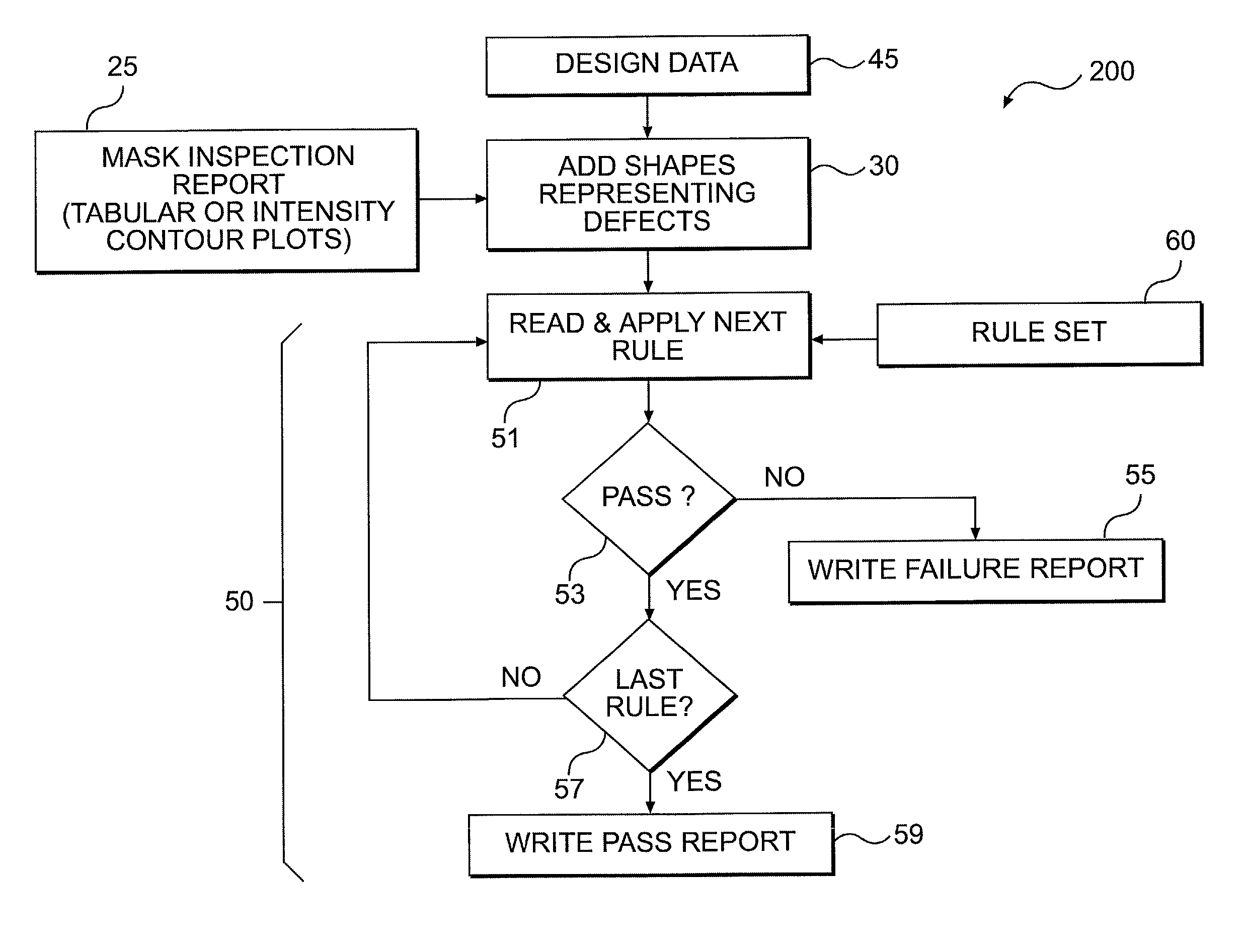
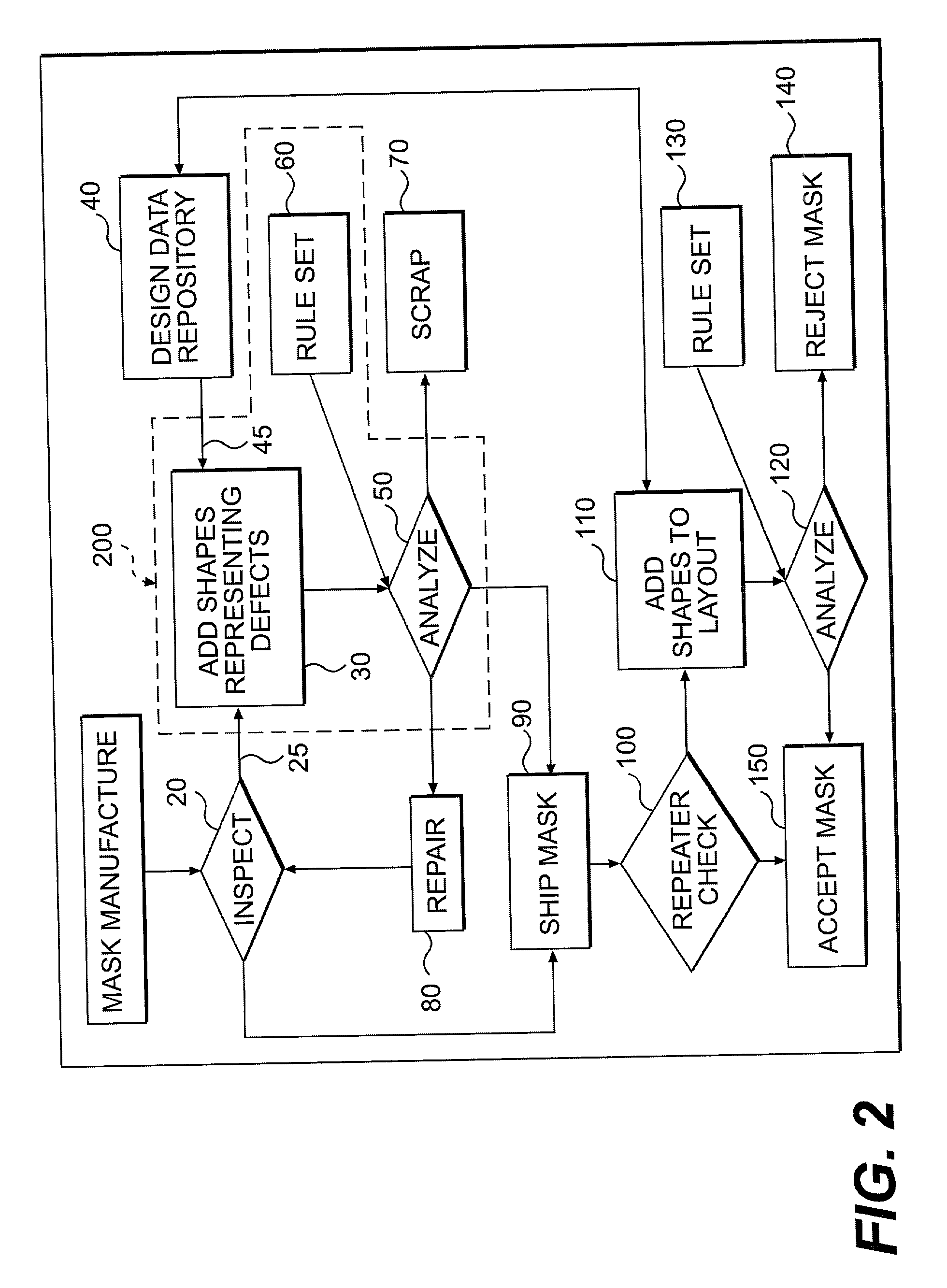
[0021]The present invention is directed to a system for analyzing defects in masks used in a semiconductor manufacturing process, and, more particularly, to a method for automating the evaluation and analysis of defects in the masks so as to determine if a given mask should be scrapped, repaired or accepted. The method utilizes defects identified through an industry-accepted inspection process and a design data repository that stores design layout data for each mask being inspected, combined with a predetermined rule set, to identify defects in the masks that would be likely to cause chip failures. By using the method of the present invention, an automated process is provided to determine whether mask defects identified during the inspection process will likely lead to failure of the product.

[0022]This method is not directed to determining whether a failure on the mask has occurred. Rather, the present invention relies on the pre-existing mask inspection process, as well as the pre-...


PUM

PropertyMeasurementUnit
sizeaaaaaaaaaa
sizeaaaaaaaaaa
sizeaaaaaaaaaa

Abstract

An automated system for analyzing mask defects in a semiconductor manufacturing process is presented. This system combines results from an inspection tool and design layout data from a design data repository corresponding to each mask layer being inspected with a computer program and a predetermined rule set to determine when a defect on a given mask layer has occurred. Mask inspection results include the presence, location and type (clear or opaque) of defects. Ultimately, a determination is made as to whether to scrap, repair or accept a given mask based on whether the defect would be likely to cause product failure. Application of the defect inspection data to the design layout data for each mask layer being inspected prevents otherwise acceptable wafer masks from being scrapped when the identified defects are not in critical areas of the mask.

Description

BACKGROUND OF THE INVENTION[0001]1. Field of the Invention[0002]The present invention generally relates to the field of semiconductor manufacturing, and, more particularly, to a method for automating the evaluation and analysis of defects in masks used in the semiconductor manufacturing process to determine which defects would cause product failure.[0003]2. Background Description[0004]As technology in the computer manufacturing field matures, the physical size of semiconductor chips continues to decrease dramatically. Accordingly, increasingly precise techniques and tools are required to manufacture the chips and the circuitry that is to be packaged on the chips. These techniques include the use of masks to create the circuit pattern corresponding to the chip design. It is a common practice in the industry to use masks in the manufacturing process for semiconductor chips. The design and layout of the circuit for the chip can be stored in the form of a mask, which can then be transfe...

Claims


Application Information

Patent Timeline
Patent Type & Authority Patents(United States)
IPC IPC(8): G06K9/00G03F1/84
CPCG03F1/84
Inventor BRUCE, JAMES A.BULA, ORESTCONRAD, EDWARD W.LEIPOLD, WILLIAM C.HIBBS, MICHAEL S.KRUEGER, JOSHUA J.
Owner IBM CORP
Why Eureka
Try Eureka