Semiconductor integrated circuit

Inactive Publication Date: 2007-10-18
PANASONIC CORP
View PDF8 Cites 27 Cited by
  • Summary
  • Abstract
  • Description
  • Claims
  • Application Information

AI Technical Summary

Benefits of technology

[0016]According to the above aspects, when the test circuit capable of being shared within the wafer is arranged outside the chip, not inside the chip, and the wiring is connected to each chip, the single test circuit can test all the chips, reducing the chip cost. Further, this enables control on the chips at one time, enabling the test to be performed in parallel to reduce the test cost.
[0017]In another semiconductor integrated circuit of the present invention, an auxiliary test device and a wiring group for sharing test circuits of a plurality of chips are formed on a wafer. In the case where a test circuit of a to-be-tested chip is out of order, a desired test is performed with the use of a test circuit of a non-target chip, eliminating chip failure caused due to a defective test circuit to improve the chip yield.
[0018]Referring to a semiconductor integrated circuit according to one embodiment of the present invention, an external test circuit and test input/output signal group repeater blocks for relaying test input/output signal wiring groups between a plurality of chips are formed on a wafer. Repeater buffers or pipeline flip-flops in the repeater blocks formed on the wafer suppress attenuation in signal level of the test input/output signal wiring groups between the external test circuit and the plurality of to-be-tested chips or suppress generation of high-frequency set up error. Further, the external test circuit can perform a low frequency or high frequency test on a plurality of

Problems solved by technology

A recent increase in scale of semiconductor integrated circuits, however, extends a test time to increase the rate of the test cost occupying the product cost.
The burn-in device has a limited number of signals usable for inputting and outputting a test pattern.
With a smaller number of usable terminals, the test itself cannot prove whether or not all of the semiconductor integrated circuits operate normally.
Further, the test circuit, which is unnecessary in a normal operation, is included in each chip, leading to an undesired increase in chip cost.
This conventional technique, however, invites an increase in an enormous number of wirings for the test to increase the wiring length and the wiring area in the isolation region, and therefore, problems, such as signal delay, reduction in

Method used


Image

  • Semiconductor integrated circuit
  • Semiconductor integrated circuit
  • Semiconductor integrated circuit

Examples


Example

[0052]Embodiments of the present invention will be described below with reference to the accompanying drawings.

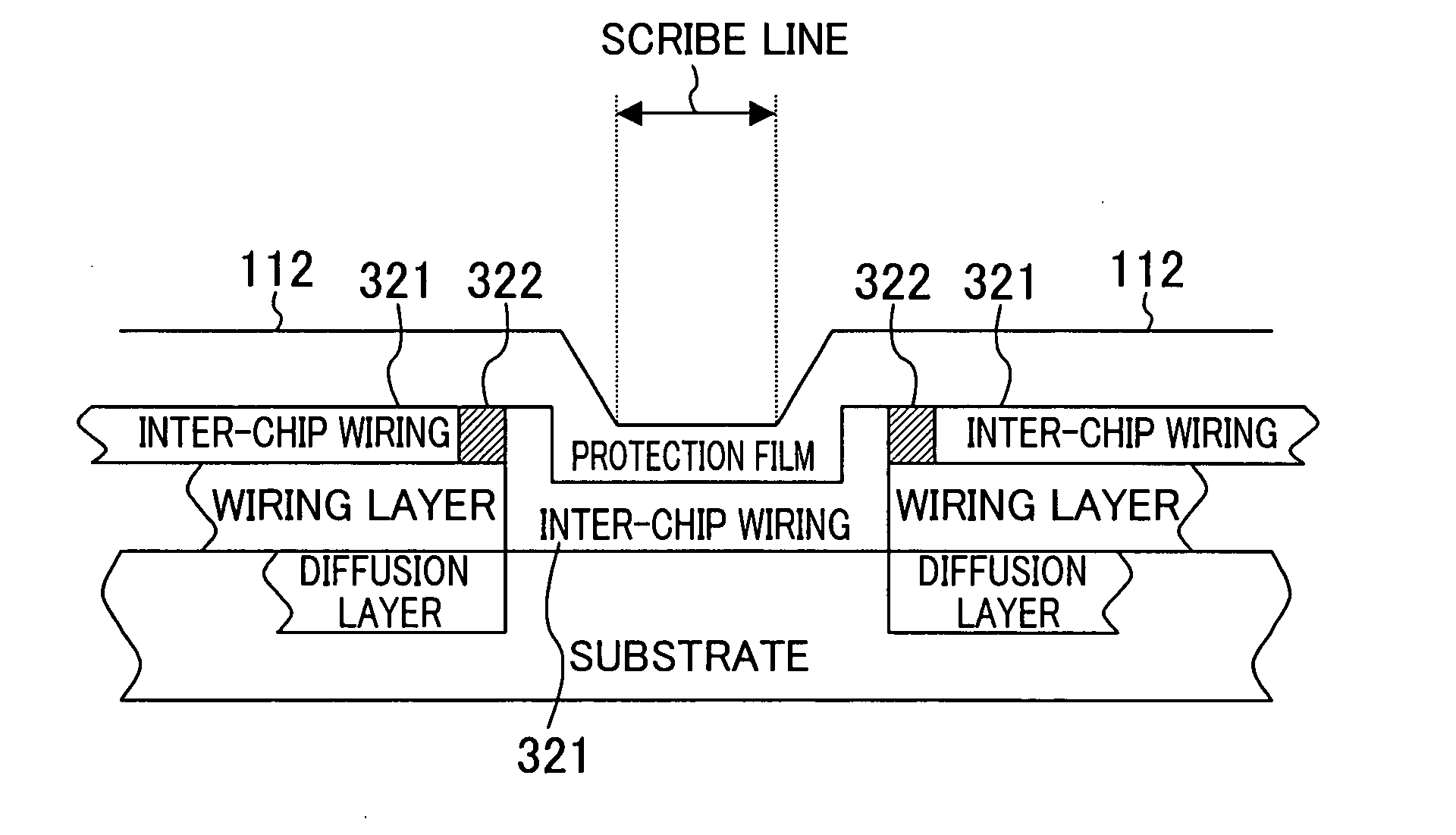
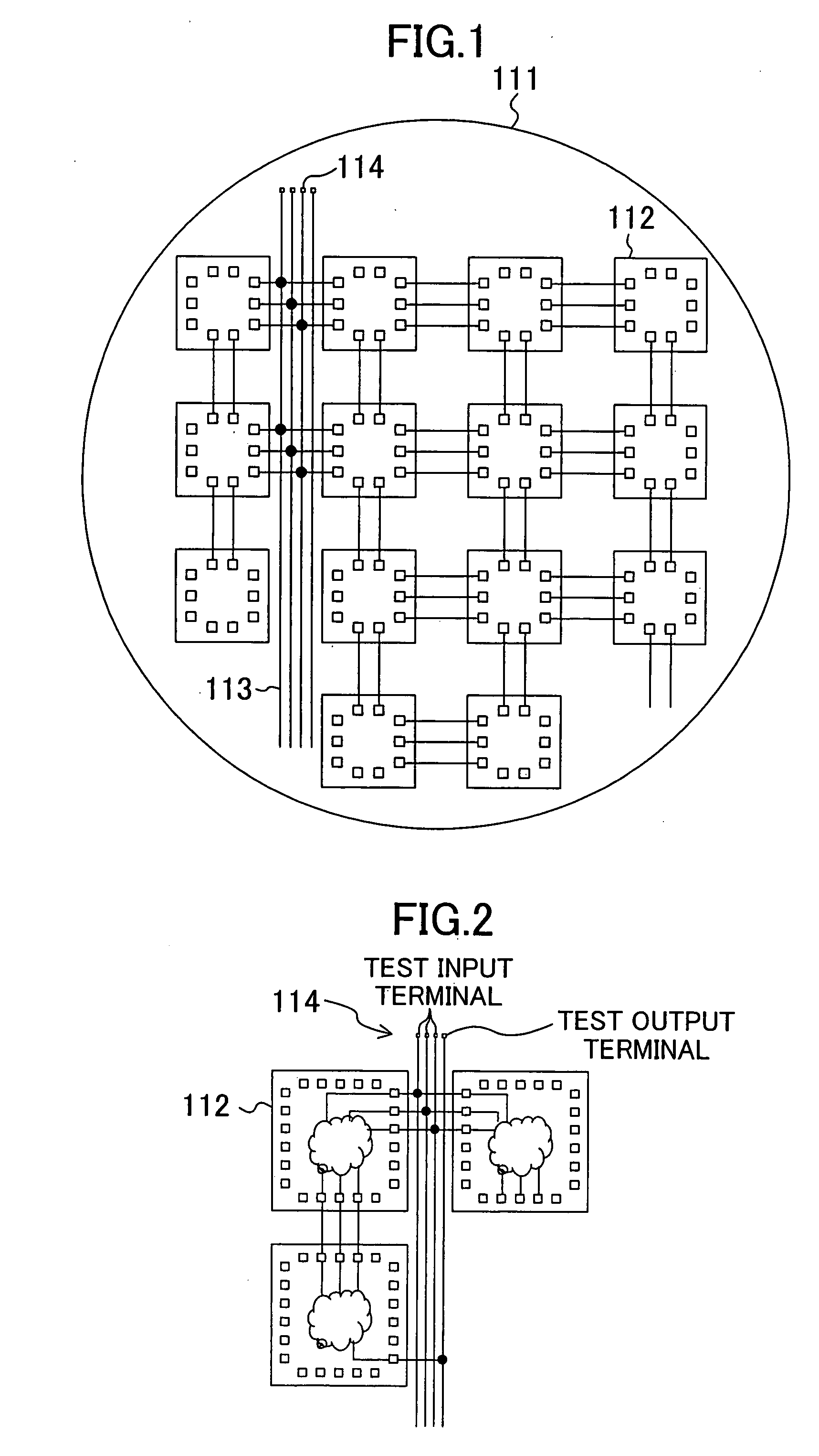
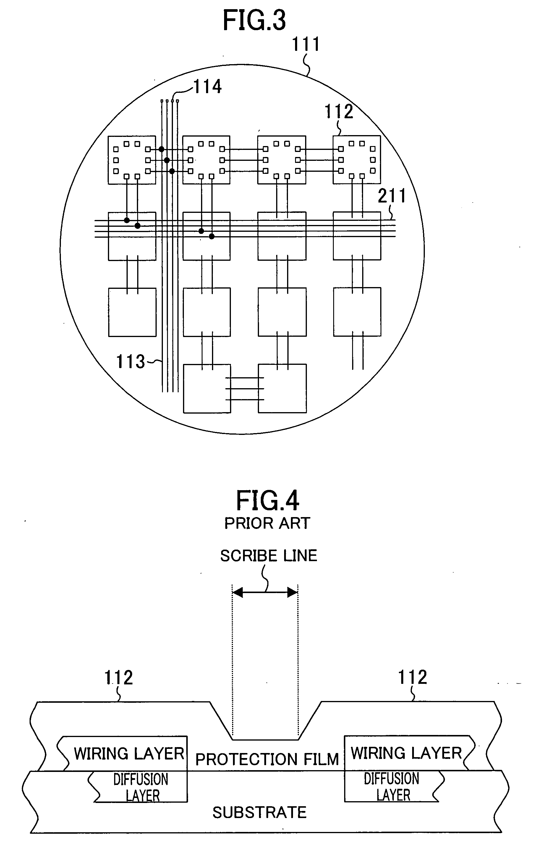
[0053]FIG. 1 is a plan view of a wafer of a semiconductor integrated circuit in one embodiment of the present invention. Wirings, which are led out from test terminals of a plurality of chips 112 formed on a semiconductor wafer 111 to the outside of the chips, are all connected to the wafer 111. A test signal wiring group 113, which is formed along a scribe line, is connected to a test terminal group 114 provided in the peripheral part of the wafer 111.

[0054]FIG. 2 shows a connection of one 112 of the chips to other adjacent chips. Test input terminals (for example, a clock input terminal, a scan enable input terminal, a scan-in terminal) in the test terminal group 114 are connected to test input terminals of a plurality of chips 112. Test output terminals (for example, a clock output terminal, a scan enable output terminal, a scan-out terminal) of the chip 112 are connecte...


PUM


Abstract

A semiconductor integrated circuit includes a wiring capable of connecting a plurality of chips on a wafer and has a configuration which is capable of cutting the wiring electrically and which allows all the chips to be tested at one time. Specifically, an exclusive test circuit region capable of being shared for testing the plurality of chips is formed on the wafer, and a test circuit is removed from each chip. Terminals of the chips and a terminal of the test circuit are connected through a wiring on the wafer or a device outside the wafer to enable a general test to be performed in burn-in.

Description

BACKGROUND OF THE INVENTION[0001]The present invention relates to a semiconductor integrated circuit and particularly relates to a test for a wafer-level semiconductor integrated circuit.[0002]Semiconductor integrated circuits are subjected to various tests, such as a probe test in a wafer level, a final test after packaged with the wafer divided, a burn-in test for degrading transistors that are going to be out of order by operating the transistors in adverse environment, a test thereafter, and so on.[0003]In the probe test and the final test, semiconductor integrated circuits packaged or on a wafer are tested one by one with the use of a test circuit included in each of the semiconductor integrated circuits. A recent increase in scale of semiconductor integrated circuits, however, extends a test time to increase the rate of the test cost occupying the product cost.[0004]Further, in the burn-in test, the semiconductor integrated circuits are operated under a condition of high tempe...

Claims


Application Information

Patent Timeline
IPC IPC(8): G01R31/02
CPCG01R31/2884H01L22/32
Inventor KAMITAI, TSUNETOMOFUJIMURA, KATSUYAKITAMOTO, DAIJUTAGUCHI, HIROFUMIHAMAGUCHI, KASUMITOKUSHIGE, TAKAHISA
Owner PANASONIC CORP
Why Eureka
Try Eureka