Light transmission touch panel and manufacturing method thereof

a technology of touch panel and light transmission, which is applied in the direction of electric digital data processing, instruments, computing, etc., can solve the problems of poor wear resistance, corrosion resistance and transparency of glass substrate, and is not suitable for touch control monitor input devices,

Inactive Publication Date: 2007-10-18
RITFAST CORP
View PDF11 Cites 196 Cited by
  • Summary
  • Abstract
  • Description
  • Claims
  • Application Information

AI Technical Summary

Problems solved by technology

Because the transparent film 111 is a flexible plastic substrate, the wear-resistance, corrosion-resistance and transparency of it are inferior to those of a glass substrate.
However, there are a plurality of opaque metal cathodes and opaque metal anodes regularly disposed on a plastic substrate to form such a capacitance circuit structure, and hence it is not suitable for the touch-control monitor as an input device.
The non-press-type touch panel is limited to have the application of a pointing device for a general computer.
Though the non-press-type touch panel is superior to the press-type touch panel in the reliability and sensitivity of operation, it cannot be popularly applied to the other electrical apparatus as an input device.

Method used


Image

  • Light transmission touch panel and manufacturing method thereof
  • Light transmission touch panel and manufacturing method thereof
  • Light transmission touch panel and manufacturing method thereof

Examples


Embodiment Construction

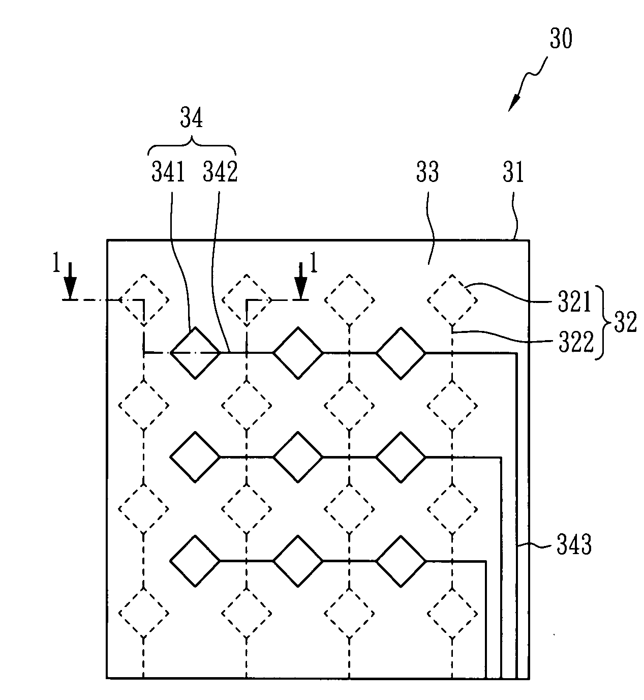
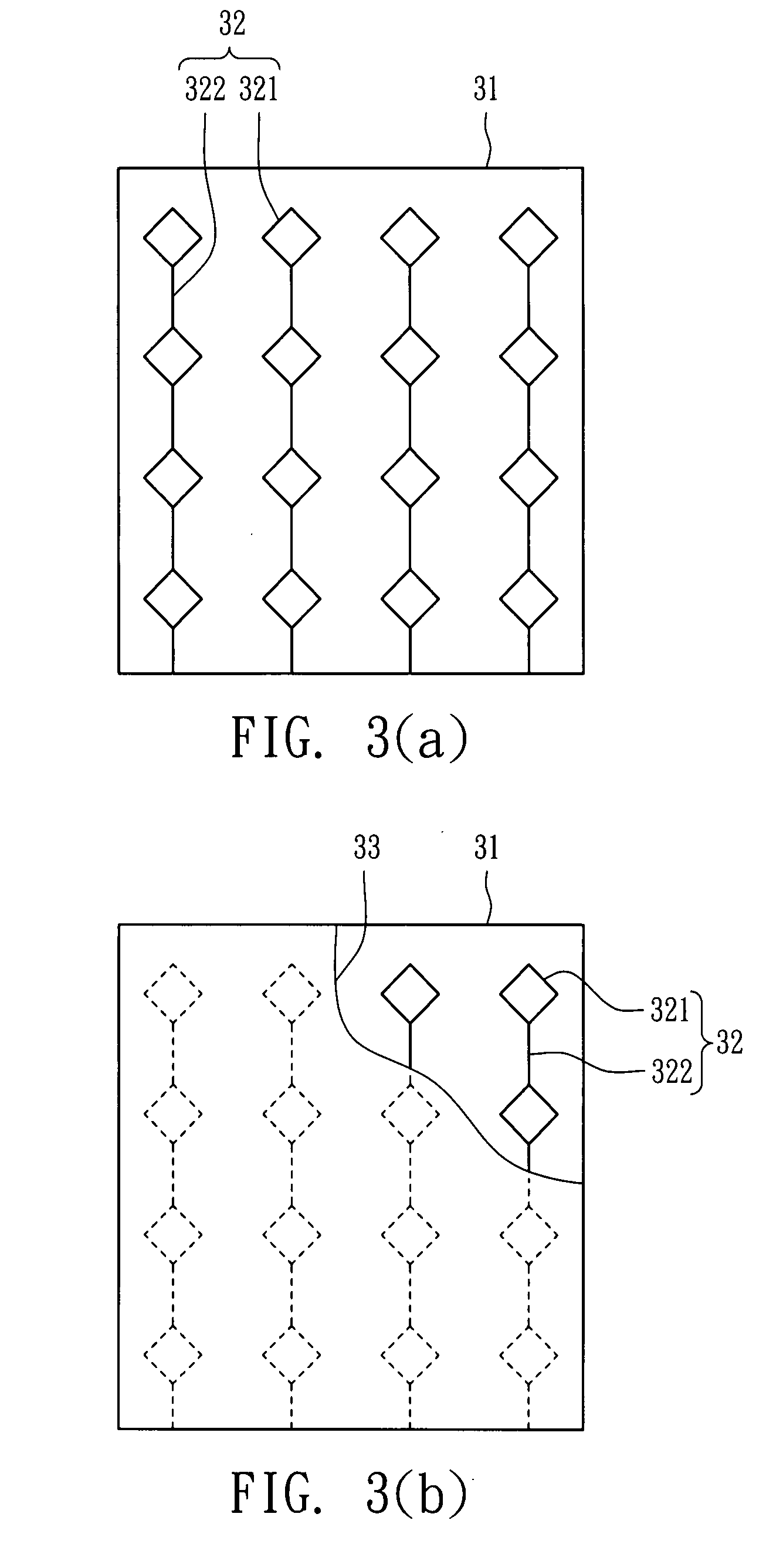
[0020]FIGS. 3(a)-3(c) are diagrams regarding the manufacturing steps of a light transmission touch panel 30 in accordance with the present invention. A first transparent conductive layer 32 is patterned and formed on a transparent substrate 31 by a photolithography process, and includes a plurality of first electrode plates 321 and a plurality of first wires 322 longitudinally connecting first electrode plates 321 that are aligned. The transparent substrate 31 is glass or a transparent polymer such as polycarbonate (PC) and polyvinyl chloride (PVC). Furthermore, the first transparent conductive layer 32 is an indium-tin oxide (ITO), aluminum-zinc oxide (AZO) or indium-zinc oxide (IZO). The photolithography process includes sputter, coating, exposure, soft baking, hard baking, development, baking and so on.

[0021]As shown in FIG. 3(b), an insulation layer 33 is overlaid on the first transparent conductive layer 32 and the substrate 31, and is a polymer material such as epoxy, polyimid...


PUM


Abstract

A light transmission touch panel comprises a transparent substrate, a first transparent conductive layer, an insulation layer and a second transparent conductive layer, wherein the first transparent conductive layer, the insulation layer and the second transparent conductive layer are patterned and overlaid on a surface of the substrate. The first transparent conductive layer and the second transparent conductive layer are either on a surface or respectively on two opposite surfaces of the insulation layer. An electrical field having a component along the surface of the substrate occurs between two adjacent portions of the first transparent conductive layer and the second transparent conductive layer once they are electrically charged. When an article touches the touch panel, the intensity of the electrical lines is accordingly changed so that the touch panel can detect where the touch position is.

Description

BACKGROUND OF THE INVENTION[0001]1. Field of the Invention[0002]The present invention relates to a light transmission touch panel and a manufacturing method thereof, and more particularly, to a touch panel having capacitance circuits and the fabricating method of such a touch panel.[0003]2. Description of the Related Art[0004]When the need for interactive functions grows, a user gradually replaces a mouse or a keyboard with a touch panel. Because the touch panel is a simple, user-friendly and space-saving input apparatus, it is generally applied to a tourist-guiding system, an automatic teller machine (ATM) and a personal assistant pad (PDA), an industrial control system, and so on.[0005]The user just touches a desired sign or a desired item displaced on the screen by a finger so as to operate the computer online connected to the touch panel. As shown in FIG. 1, a touch-control monitor 10 has a transparent touch panel 11 placed on the surface of an electrical screen 12 that shows se...

Claims


Application Information

Patent Timeline
Patent Type & Authority Applications(United States)
IPC IPC(8): G06F3/041
CPCG06F2203/04111G06F3/044G06F3/0445G06F3/0446
Inventor CHANG, YIHTANG, TUNG-YANGLAI, YUANG-WEIKUO, CHUN-CHIEHCHEN, CHING-LUNG
Owner RITFAST CORP
Why Eureka
Try Eureka