

Method of manufacturing a through electrode
a technology of through electrodes and electrodes, applied in the direction of semiconductor devices, semiconductor/solid-state device details, electrical apparatus, etc., can solve the problems of reducing the contact resistance between electrodes, and achieve the effect of excellent properties
Inactive Publication Date: 2007-10-18
RENESAS ELECTRONICS CORP
View PDF18 Cites 19 Cited by
- Summary
- Abstract
- Description
- Claims
- Application Information
AI Technical Summary
Benefits of technology
The design enhances adhesion and conductivity between the bump and the plug, reduces contact resistance, and simplifies the manufacturing process, thereby improving the reliability and reducing parasitic capacitance of the through electrode.
Problems solved by technology
Further, the electrical contact between the bump and the through plug is fully secured, which leads to decrease of contact resistance therebetween.
Method used
View moreImage
Smart ImageViewing Examples

Examples
example
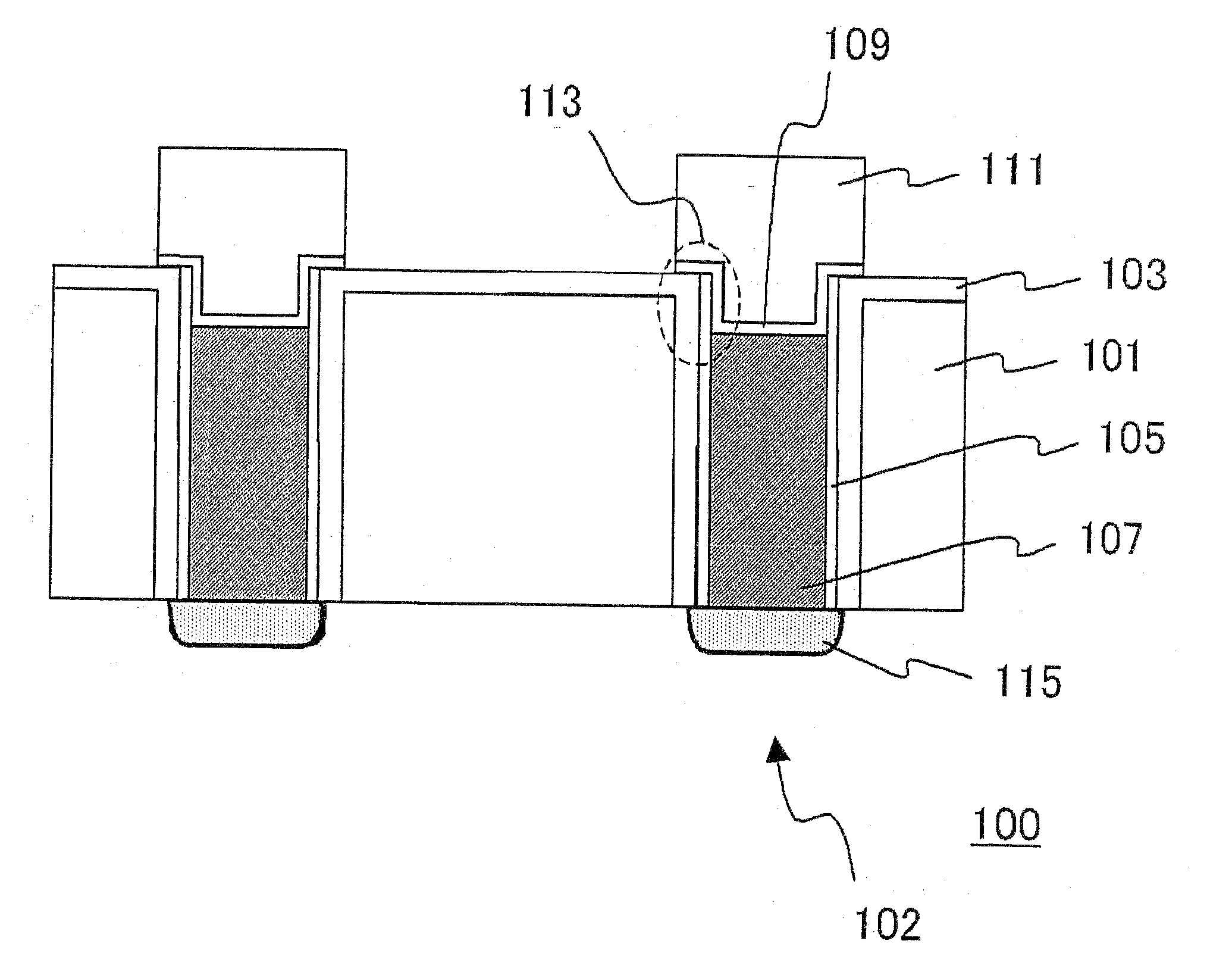
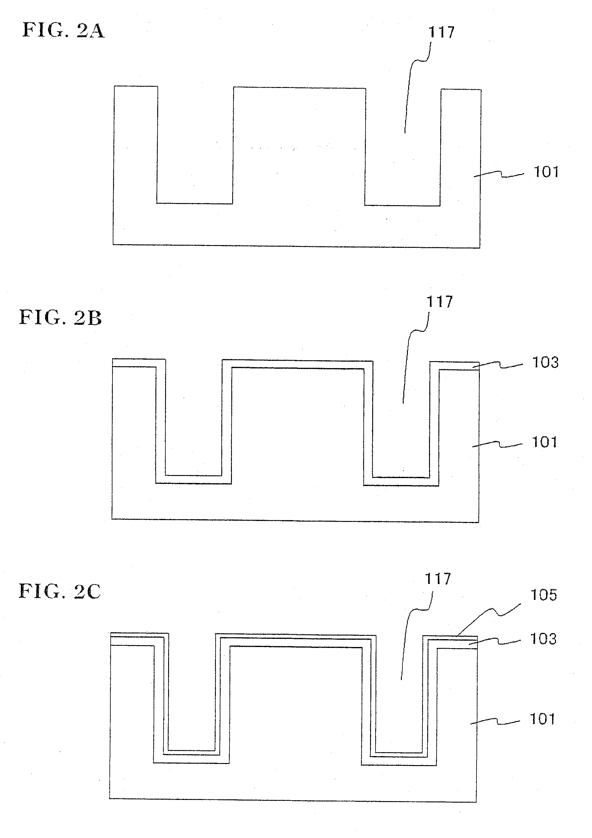
[0085] As the example, the silicon spacer 100 shown in FIG. 1 was manufactured according to the process described referring to FIGS. 2A to 2C, 3D to 3F, 4G to 4H and 5I. Here, a SiO2 film of 300 nm in thickness was formed as the insulative thick film 103. The SiN film 105 was formed to have a thickness of 50 nm. The through plug 107 was formed of a Cu film. Also, the silicon substrate 101 was thinned to 200 μm by grinding rear surface of the silicon substrate 101. The silicon spacer 100 including the through electrode 102 was obtained with highly stability of the manufacturing process and an excellent yield.
Login to View More PUM
| Property | Measurement | Unit |
|---|---|---|
| thickness | aaaaa | aaaaa |
| thickness | aaaaa | aaaaa |
| thickness | aaaaa | aaaaa |
Abstract
A through electrode that offers excellent performance and can be manufactured through a simple process is to be provided. In a silicon spacer including a silicon substrate, an insulative thick film is provided so as to be in contact with a surface of the silicon substrate and a side wall of a through hole penetrating the silicon substrate. An upper surface of a through plug is retreated to a lower level than an interface between the silicon substrate and the insulative thick film, thus to define a height gap. A first bump is then formed, which is connected to the retreated surface of the through plug and has a larger diameter than that of the through plug at the upper surface of the insulative thick film.
Description
[0001] This application is based on U.S. patent application Ser. No. 11 / 092,403 filed Mar. 30, 2005 and Japanese patent application No. 2004-099681, the content of which is incorporated hereinto by reference. BACKGROUND OF THE INVENTION [0002] 1. Field of the Invention [0003] The present invention relates to a through electrode, a spacer provided with the through electrode, and a method of manufacturing them. [0004] 2. Related Art [0005] In recent years, with the view of achieving an even higher degree of integration of a semiconductor chip, development of three-dimensional implementation of semiconductor chips such as an LSI has lately been vigorously carried out. Such attempts include providing a through electrode on a semiconductor substrate. An example of the through electrode is disclosed in the H. Yonemura, et al., “Time-Modulated Cu-Plating Technique for Fabricating High-Aspect-Ratio Vias for Three-dimensional Stacked LSI System”, 2002, Proceedings of the International Interc...
Claims
Login to View More Application Information
Patent Timeline
 Patent Type & AuthorityApplications(United States)
IPC IPC(8): H01L21/44H01L23/52H01L21/28H01L21/3205H01L21/48H01L21/768H01L23/14H01L23/32H01L23/48H01L25/065
CPCH01L21/6835H01L21/76898H01L2224/04042H01L2224/0554H01L2224/05001H01L2224/05555H01L2224/73265H01L2224/32225H01L24/48H01L2924/30105H01L2924/15311H01L2924/1433H01L2924/04953H01L2924/01082H01L23/147H01L23/481H01L24/03H01L24/05H01L24/11H01L24/12H01L24/73H01L25/0657H01L2221/68372H01L2224/03912H01L2224/0401H01L2224/1147H01L2224/13009H01L2224/13022H01L2224/13025H01L2224/13099H01L2224/13144H01L2224/16H01L2224/48227H01L2224/73207H01L2225/0651H01L2225/06513H01L2225/06572H01L2924/01004H01L2924/01005H01L2924/01006H01L2924/01013H01L2924/01014H01L2924/01015H01L2924/01022H01L2924/01028H01L2924/01029H01L2924/01033H01L2924/0105H01L2924/01073H01L2924/01078H01L2924/01079H01L2924/00012H01L2924/00H01L2924/00014H01L2224/45099H01L2224/45015H01L2924/207
InventorKOMURO, MASAHIRO
OwnerRENESAS ELECTRONICS CORP