Image sensor with built-in thermometer for global black level calibration and temperature-dependent color correction

a technology of image sensor and thermometer, which is applied in the field of black level calibration and temperature-dependent color correction of semiconductor imager, can solve the problems of noise sources only affecting specific portions of the sensor array, distortion of the resulting digital image, and the entire sensor array

Inactive Publication Date: 2007-11-29
APTINA IMAGING CORP
View PDF16 Cites 75 Cited by
  • Summary
  • Abstract
  • Description
  • Claims
  • Application Information

AI Technical Summary

Problems solved by technology

However, various noise sources can affect individual pixel outputs and thus distort the resulting digital image.
Some noise sources may affect the entire sensor array, thereby requiring frame-wide correction of the pixel output from the array.
Other noise sources may only affect specific portions of the sensor array.
For example, row-specific noise may be generated from a mismatch of circuit structures in the image sensors due to variations in manufacturing processes.
The effect of row-specific noise in an image se...

Method used


Image

  • Image sensor with built-in thermometer for global black level calibration and temperature-dependent color correction
  • Image sensor with built-in thermometer for global black level calibration and temperature-dependent color correction
  • Image sensor with built-in thermometer for global black level calibration and temperature-dependent color correction

Examples


Embodiment Construction

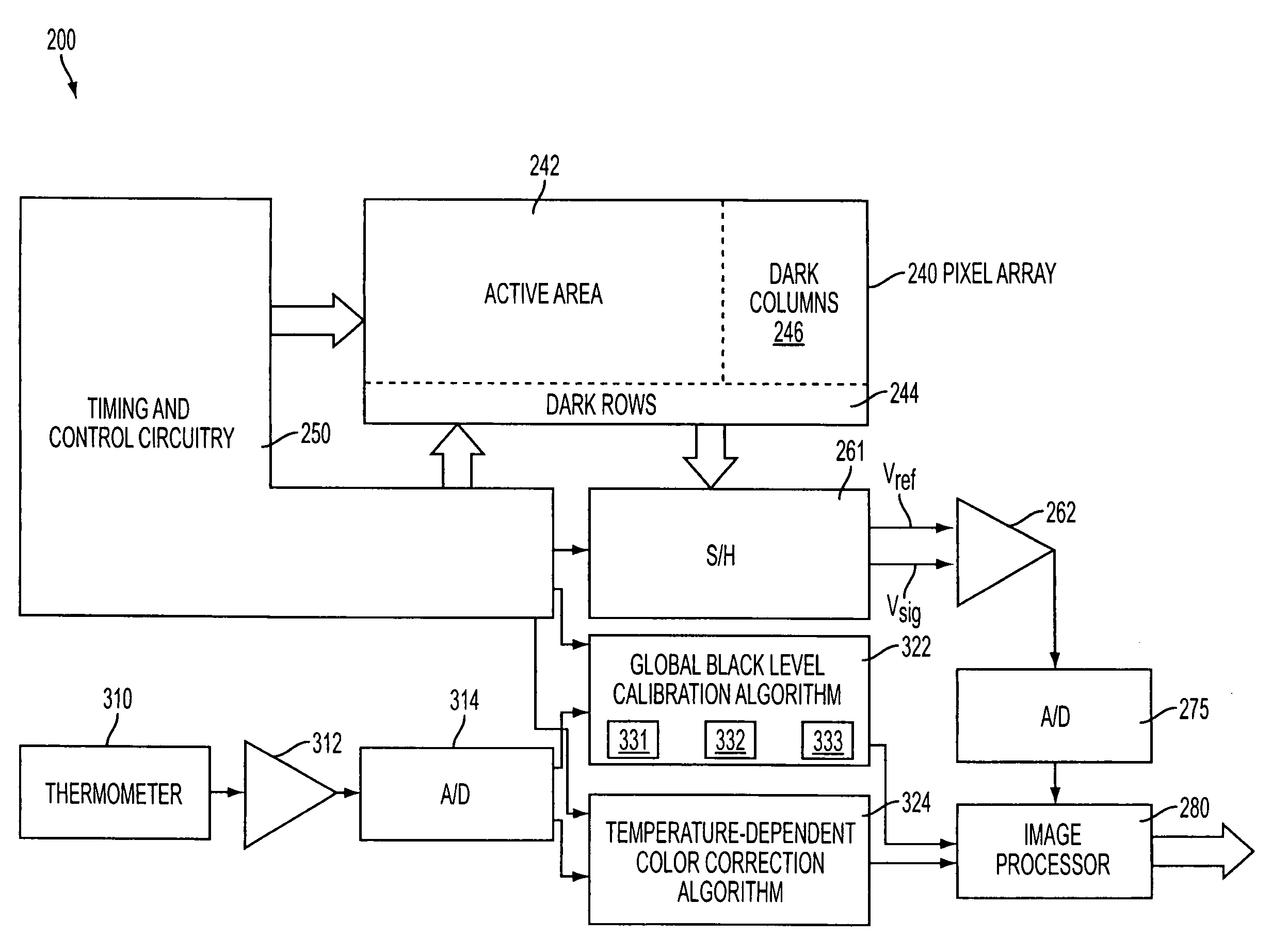
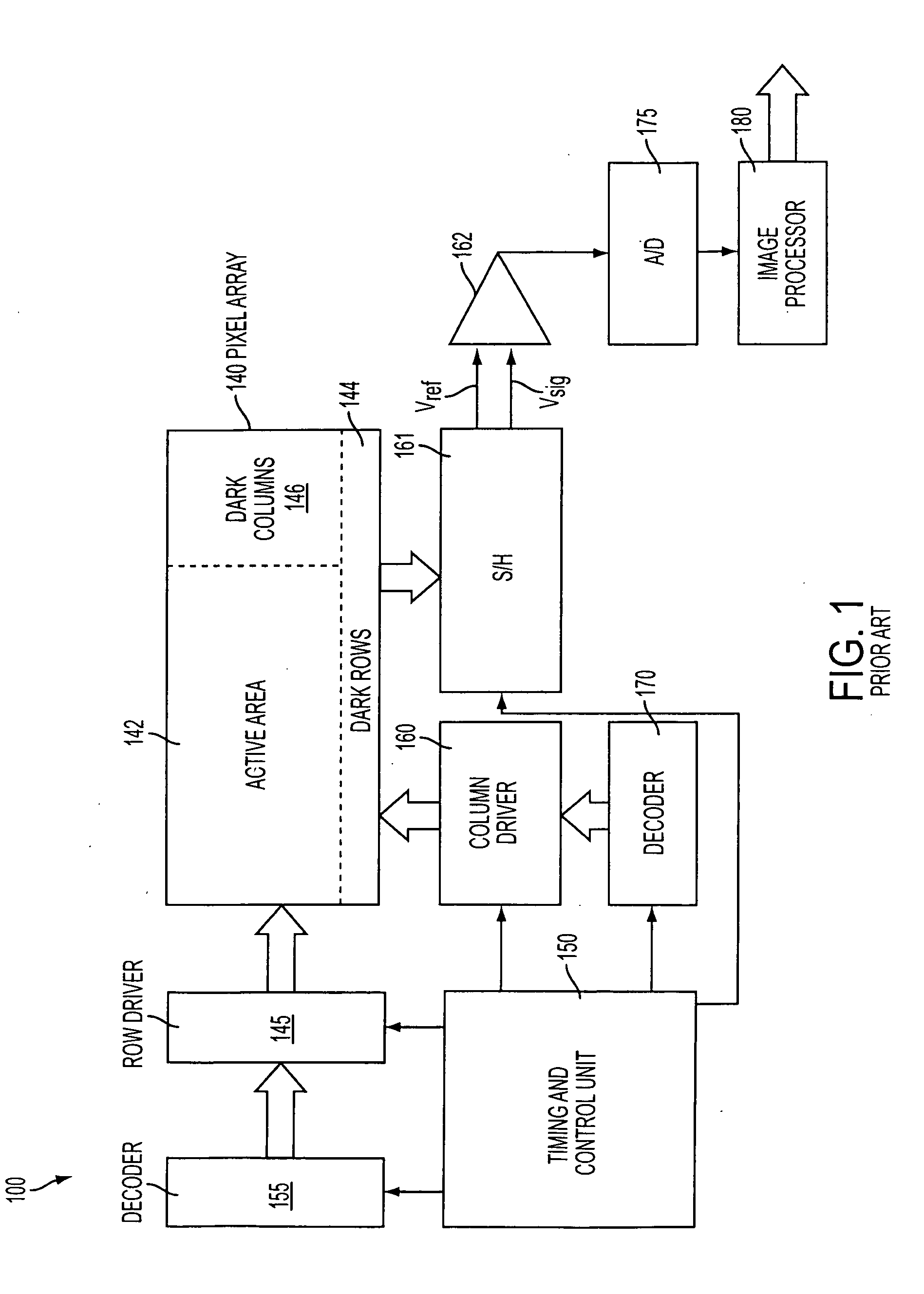
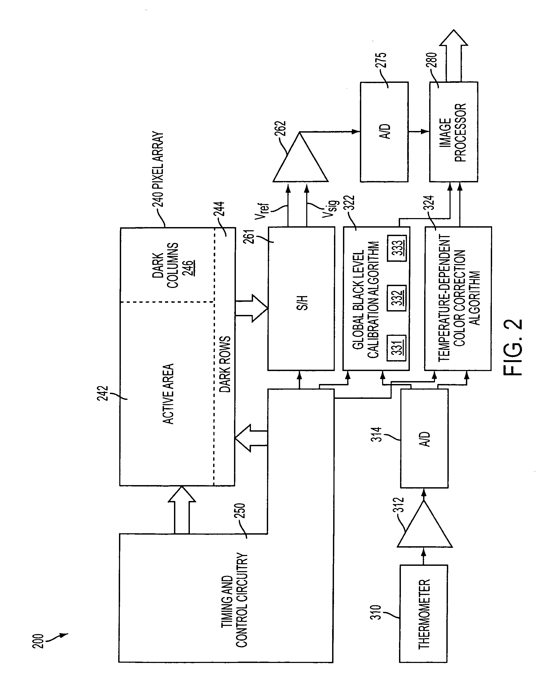
[0014]One method that has been used in response to the disadvantages of using optically black pixels to set the black level value, as explained above, has been to tie the photodiode of some or all pixels in the dark rows 144 (FIG. 1) to a fixed voltage, as presented in U.S. patent application Ser. No. 11 / 066,781. The fixed voltage is, in essence, a fixed black level for the pixel array 140. The advantages of this method is that the black level calculation is not influenced by blooming, IR reflections, etc., and that every frame utilizes a constant and unchanging black level. However, tied pixels are not sensitive to any changes in dark current due to temperature. Thus, a black level generated by utilizing tied pixels may not accurately compensate for the noise caused by temperature dependent dark current.

[0015]The noise generated by thermal-induced dark current can be calculated and compensated for by directly measuring the temperature of an image sensor. In an example embodiment of...


PUM


Abstract

A semiconductor image sensor is provided that includes an on-chip temperature-sensitive element. The signal output of the temperature-sensitive element is used to determine a black level value for the image sensor and to calculate a color correction value to be applied to the signal output of the semiconductor image sensor. The signal output of the temperature-sensitive element may be determined by time-averaging a series of signal outputs from the temperature-sensitive element. The temperature-sensitive element signal output may also be determined by combining, e.g., averaging, the signal outputs of a plurality of on-chip temperature-sensitive elements.

Description

FIELD OF THE INVENTION[0001]The invention relates generally to semiconductor imagers. More specifically, the invention relates to black level calibration and temperature-dependent color correction in semiconductor imagers.BACKGROUND OF THE INVENTION[0002]Complementary metal-oxide semiconductor (CMOS) image sensors utilize sensor arrays that are composed of rows and columns of pixels. The pixels are sensitive to light of various wavelengths. When a pixel is subjected to a wavelength of light to which the pixel is sensitive, the pixel generates electrical charge that represents the intensity of the sensed light. When each pixel in the sensor array outputs electrical charge based on the light sensed by the array, the combined electrical charges represent the image projected upon the array. Thus, CMOS image sensors are capable of translating an image of light into electrical signals that may be used, for example, to create digital images.[0003]Ideally, the digital images created by CMOS...

Claims


Application Information

Patent Timeline
IPC IPC(8): H04N9/64H04B1/40H04N5/225H04N5/361
CPCH04N5/361H04N5/359H04N25/62H04N25/63
Inventor JIANG, JUTAO
Owner APTINA IMAGING CORP
Why Eureka
Try Eureka