Liquid crystal display device

a liquid crystal display and display device technology, applied in the direction of optics, non-linear optics, instruments, etc., can solve the problems of difficult control of the printing region, low viscosity of the material used in the ink jet printing method, and difficult size control of the periphery of the orientation film, etc., to reduce the region to be printed, suppress the spreading

Active Publication Date: 2007-12-06
PANASONIC LIQUID CRYSTAL DISPLAY CO LTD +1
View PDF3 Cites 25 Cited by
  • Summary
  • Abstract
  • Description
  • Claims
  • Application Information

AI Technical Summary

Benefits of technology

[0015]In forming the orientation film using the ink jet printing method, as a method which prevents the spreading by wetting of the printed material to the sealing material, for example, a method which preliminarily decreases a region to be printed by taking a spreading-by-wetting quantity of printed material into consideration may be considered. However, this method has a drawback that the method is liable to easily generate the irregularities of a film thickness of the material which is printed in the inside of the display region.
[0016]Further, as another method, for example, a method which suppresses the spreading by wetting of the printed material by increasing the viscosity of a material to be printed. However, this method has a drawback that the method is liable to generate a region which is not covered with the material by coating due to an ejection failure at the time of printing.
[0017]Accordingly, it is an object of the present invention to provide a technique which can suppress the spreading by wetting of an orientation film of a liquid crystal display panel outside a display region and, at the same time, can maintain the uniformity of the film thickness within the display region.
[0027]In the liquid crystal display device of the present invention, at least one substrate out of the pair of substrate includes the elongated groove portion which extends in the direction along the outer periphery of the display region in the substantially annular region which is arranged inside the region where the sealing material is arranged and outside the display region. Here, the groove portion is formed of recessed grooves which are formed in the insulation layer and the conductive layer which extends along side surfaces and bottom surfaces of the recessed grooves, and the conductive layer is made of the same material as the transparent electrodes. Due to such a constitution, in forming the orientation film on the display region of the substrate which includes the groove portion by printing or coating a resin material in a liquid form, even when the printed resin material in a liquid form spreads to the outside of the display region, the spreading of the resin material can be prevented by the groove portion. Accordingly, the spreading by wetting of the orientation film on the liquid crystal display panel outside the display region can be suppressed and, at the same time, the uniformity of film thickness of the orientation film within the display region can be maintained.

Problems solved by technology

However, in forming the orientation film using the ink jet printing method, it has been pointed out that a size control and a shape control of a periphery of the orientation film are difficult.
That is, in printing a material of the resin film on the substrate using the ink jet printing method, there exists a drawback that a control of a printing region is difficult.
Such a drawback is attributed to a fact that, for example, the viscosity of a material which is used in the ink jet printing method is low compared to the viscosity of a material used in the aniline printing method or the like.
When the orientation film reaches the region where the sealing material is formed, for example, the adhesiveness between the sealing material and the TFT substrate (orientation film) becomes insufficient thus giving rise to a drawback that a liquid crystal material leaks.
However, this method has a drawback that the method is liable to easily generate the irregularities of a film thickness of the material which is printed in the inside of the display region.

Method used


Image

  • Liquid crystal display device
  • Liquid crystal display device
  • Liquid crystal display device

Examples


Embodiment Construction

[0056]Hereinafter, the present invention is explained in detail in conjunction with modes for carrying out the invention (embodiments) by reference to drawings.

[0057]Here, in all drawings for explaining the embodiments, parts having identical functions are given same symbols and their repeated explanation is omitted.

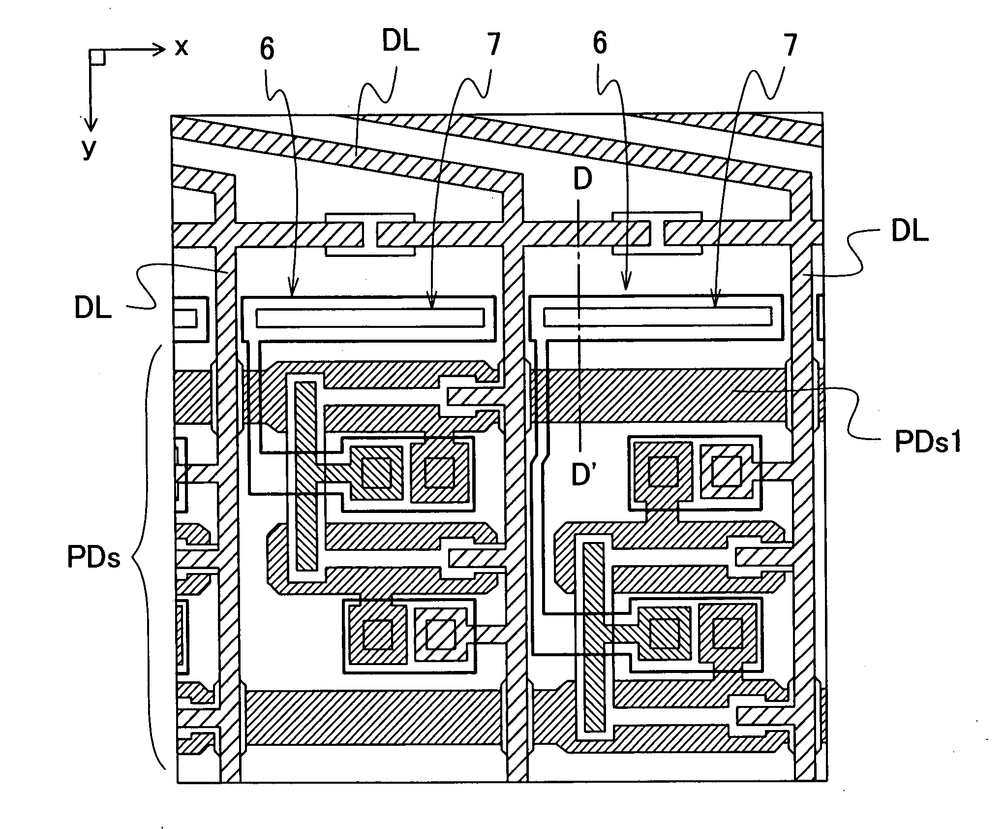
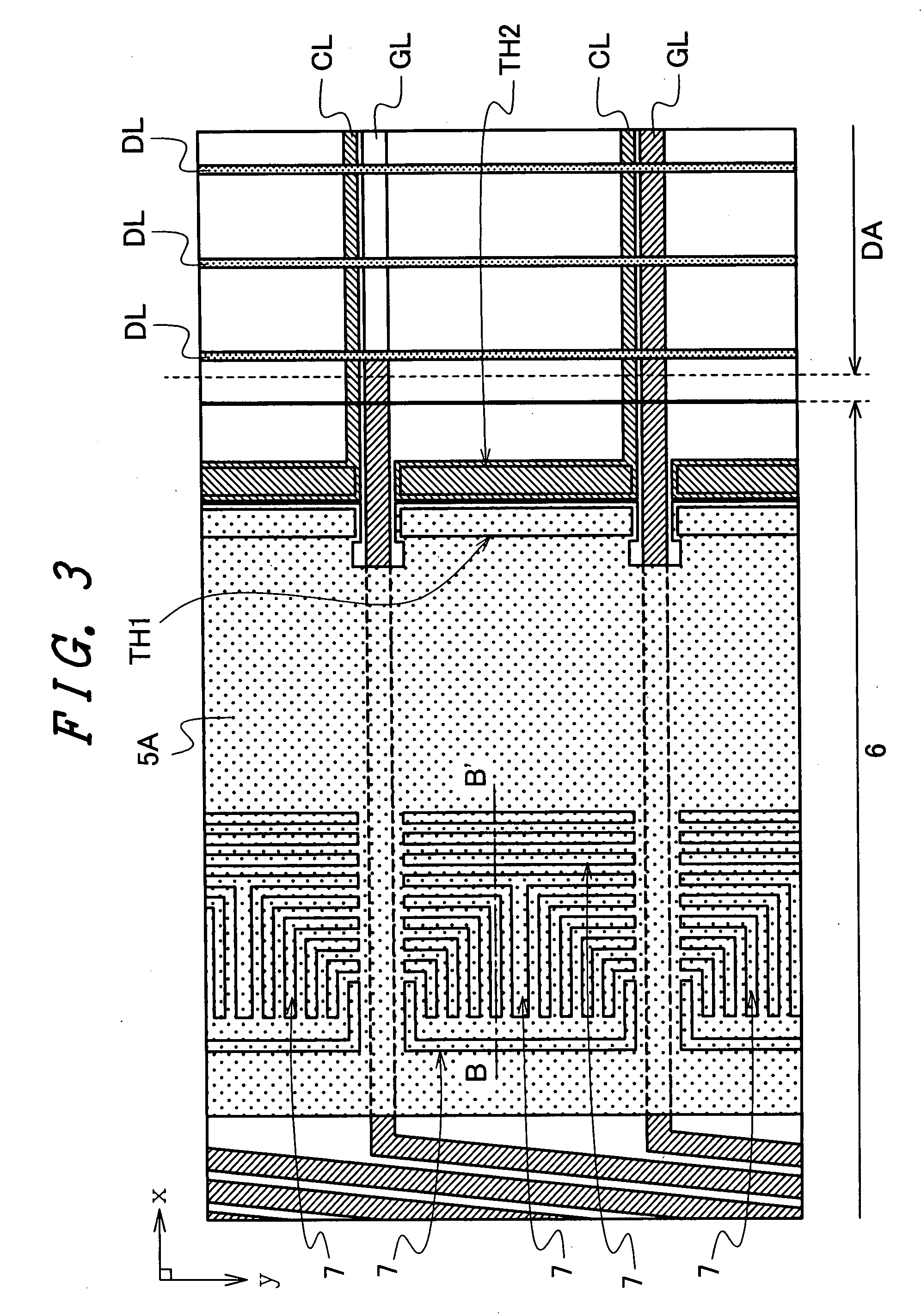
[0058]FIG. 1 is a schematic plan view showing the schematic constitution of a liquid crystal display panel of one embodiment according to the present invention. FIG. 2 is a schematic cross-sectional view taken along a line A-A′ in FIG. 1.

[0059]The display device according to the present invention is, for example, as shown in FIG. 1 and FIG. 2, a liquid crystal display device which includes a liquid crystal display panel in which an annular sealing material 3 is arranged between a pair of substrates 1, 2 and a liquid crystal material 4 is sealed in a space surrounded by the pair of substrates 1, 2 and the sealing material 3. Here, a display region DA for displaying a vide...


PUM

PropertyMeasurementUnit
conductiveaaaaaaaaaa
massaaaaaaaaaa
sizeaaaaaaaaaa

Abstract

The present invention suppresses the spreading by wetting of an orientation film of a liquid crystal display panel outside a display region and, at the same time, maintains the uniformity of film thickness of the orientation film within a display region. In a liquid crystal display device which includes a display panel which arranges a sealing material having an annular shape between a pair of substrates, seals a liquid crystal material in a space surrounded by the pair of substrates and the sealing material, the pair of substrates form orientation films on surfaces thereof opposite to surfaces thereof which face each other, the orientation films are brought into contact with transparent electrodes which are formed on surfaces of transparent substrates by way of insulation layers, at least one substrate out of the pair of substrates includes an elongated groove portion which extends in the direction along an outer periphery of the display region in a substantially annular region which is arranged inside a region where the sealing material is arranged and outside the display region, and the groove portion is formed of recessed grooves which are formed in the insulation layer and an ITO film which extends along side surfaces and bottom surfaces of the recessed grooves.

Description

[0001]The present application claims priority from Japanese application JP2006-151478 filed on May 31, 2006, the content of which is hereby incorporated by reference into this application.BACKGROUND OF THE INVENTION[0002]1. Field of the Invention[0003]The present invention relates to a liquid crystal display device, and more particularly to a technique which is effectively applicable to a control of a coating region of an orientation film.[0004]2. Description of the Related Art[0005]Conventionally, as a display device which displays a video or an image, there has been known a liquid crystal display device which uses a liquid crystal display panel sealing a liquid crystal material between a pair of substrates.[0006]In the liquid crystal display panel, on one substrate out of a pair of substrates, for example, a plurality of scanning signal lines and a plurality of video signal lines are formed. Then, a region which is surrounded by two neighboring scanning signal lines and two neighb...

Claims


Application Information

Patent Timeline
Patent Type & Authority Applications(United States)
IPC IPC(8): G02F1/1343G02F1/1333
CPCG02F2001/133388G02F1/133711G02F1/133388G02F1/1339
Inventor IWATO, HIROAKIWATANABE, YOSHIKIASHIZAWA, KEIICHIROU
Owner PANASONIC LIQUID CRYSTAL DISPLAY CO LTD
Why Eureka
Try Eureka