

Elimination of first wafer effect for pecvd films
- Summary
- Abstract
- Description
- Claims
- Application Information
AI Technical Summary
Benefits of technology
Problems solved by technology
Method used
Image

Examples
example
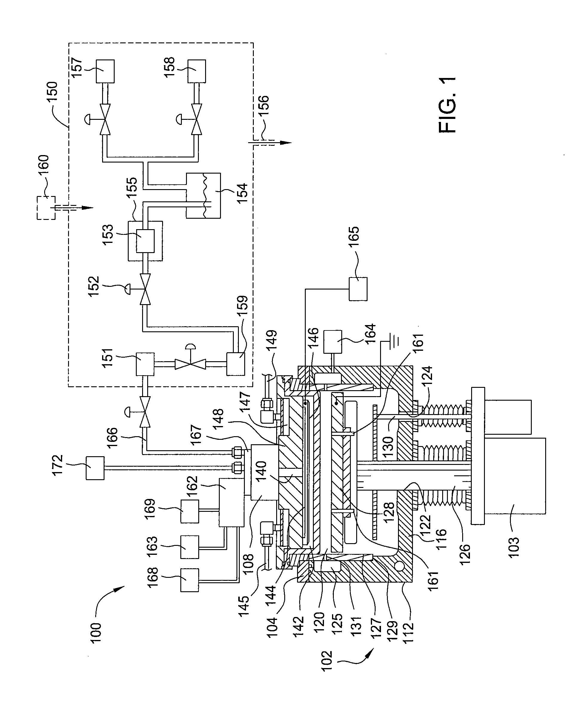
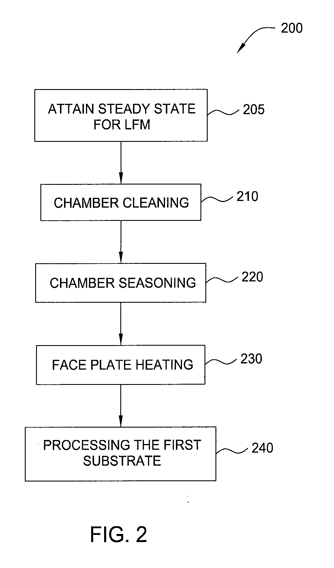
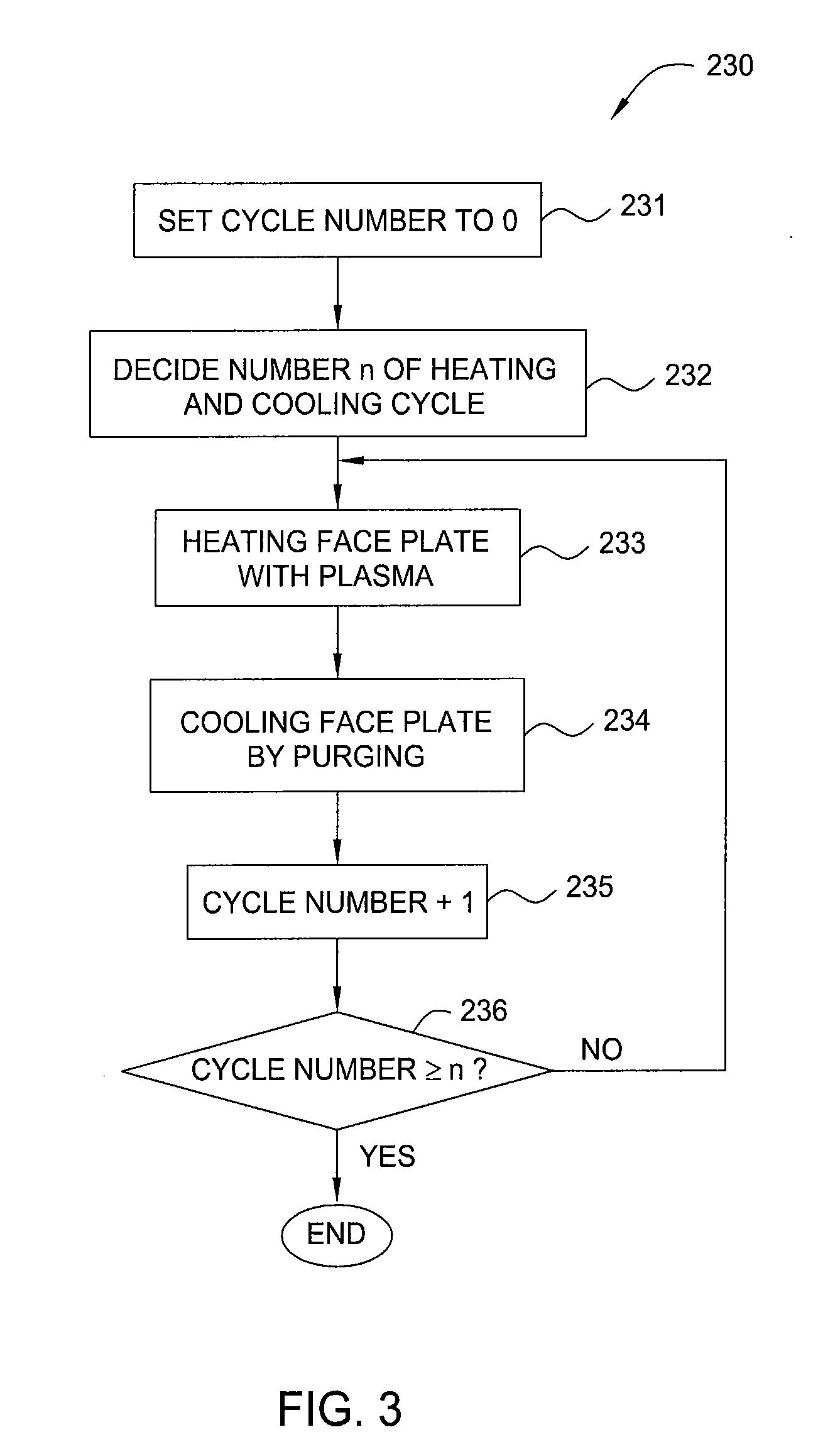
[0050]A “Start up” sequence of the present invention is performed for a PECVD deposition process for depositing a carbon doped silicon oxide film from octamethylcyclotetrasiloxane (OMCTS) using a PRODUCER® SE twin chamber, which comprises two processing chambers similar to the PECVD system 100 of FIG. 1. The detailed description of the PRODUCER® SE twin chamber may be found in U.S. Pat. No. 5,855,681 and No. 6,495,233, which are incorporated by reference herein. The carbon doped silicon oxide film is to be deposited on substrates at a chamber temperature of about 150° C.
Seasoning the Liquid Flow Meter
[0051]After the chamber being idle for a period of time, the OMCTS is flown through the system with radio frequency sources turned off for about at least 2 minutes. More particularly, OMCTS is flown through the system for about 2 minutes to about 5 minutes.
Cleaning the Chamber
[0052]A cleaning process is performed to the chamber. The cleaning time is about 3 times as long as the seasonin...
PUM
| Property | Measurement | Unit |
|---|---|---|
| Length | aaaaa | aaaaa |
| Time | aaaaa | aaaaa |
| Power | aaaaa | aaaaa |
Abstract
Description
Claims
Application Information