Display Device, Liquid Crystal Display Device, And Method For Producing A Display Device

a liquid crystal display and display device technology, applied in the direction of identification means, instruments, computing, etc., can solve the problems affecting the display quality, so as to suppress the effect of deteriorating display quality

Inactive Publication Date: 2007-12-13
SHARP KK
View PDF5 Cites 27 Cited by
  • Summary
  • Abstract
  • Description
  • Claims
  • Application Information

AI Technical Summary

Benefits of technology

[0028] The present invention has been made in view of the problem described above, and has an object to make it possible to fix a broken display wire when a wire breakage occurs, in such a manner that the decrease in the display quality is suppressed, irrespective of the wire breakage position.

Problems solved by technology

Therefore, if a wire breakage occurs in a display wire such as a gate line or a source line in an active matrix-type liquid crystal display device, the display signal from the driver circuit is not supplied to the display wire beyond the wire breakage position, thus significantly deteriorating the display quality.
However, in an actual liquid crystal display device, it is not possible to know where a wire breakage of the source line 102 will occur.
Thus, the display quality deteriorates.
However, if the resolution is high (e.g., UXGA), the charging time is short and the overshoot or undershoot will be non-negligible.
Thus, with the recent increase in the resolution and the screen size of a liquid crystal display device, the difference between the load on a normal source line and the load on a source line divided in a wire breakage further increases, thereby increasing the overshoot or undershoot and deteriorating the display quality.

Method used


Image

  • Display Device, Liquid Crystal Display Device, And Method For Producing A Display Device
  • Display Device, Liquid Crystal Display Device, And Method For Producing A Display Device
  • Display Device, Liquid Crystal Display Device, And Method For Producing A Display Device

Examples


embodiment 1

[0100] A liquid crystal display device 50 according to Embodiment 1 of the present invention will now be described.

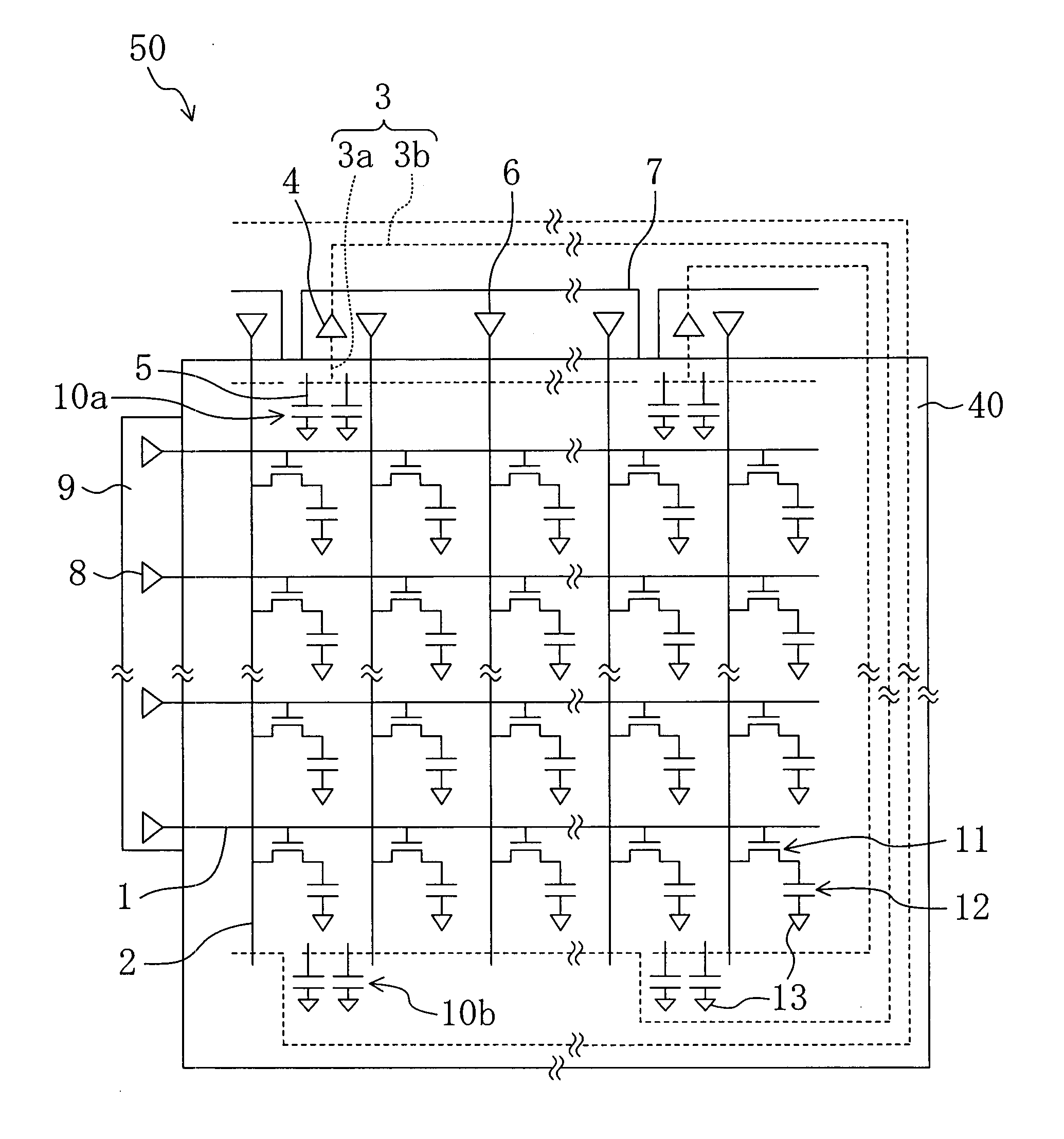
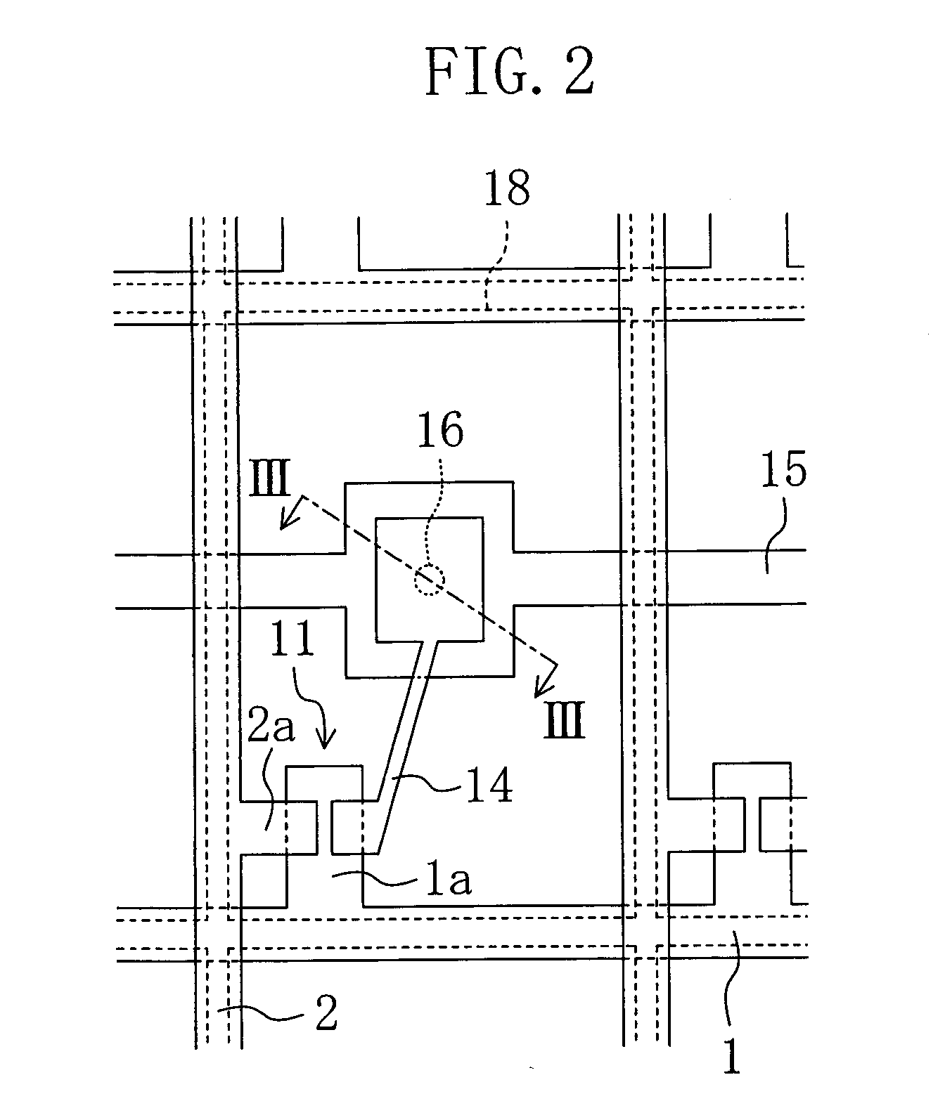
[0101]FIG. 1 is an equivalent circuit diagram showing the liquid crystal display device 50 according to Embodiment 1 of the present invention. FIG. 2 is a plan view showing a single pixel of the liquid crystal display device 50, and FIG. 3 is a cross-sectional view taken along line III-III of FIG. 2.

[0102] The liquid crystal display device 50 includes a liquid crystal display panel 40, a gate driver 9 provided along the left side of the liquid crystal display panel 40, and a source driver 7 provided along the upper side of the liquid crystal display panel 40.

[0103] The liquid crystal display panel 40 includes an active matrix substrate, a counter substrate provided so as to oppose the active matrix substrate, and a liquid crystal layer 12 interposed between the substrates.

[0104] The active matrix substrate includes, on a glass substrate 20, a plurality of gate lines...

embodiment 2

[0192] The present invention may employ the following configuration for Embodiment 1 as described above. In this and subsequent embodiments, like elements to those shown in FIG. 1 to FIG. 10 will be denoted by like reference numerals and will not be further described below.

[0193] In Embodiment 1, the first electrodes 10c of a plurality of first spare capacitors 10a and the first electrodes 10c of a plurality of second spare capacitors 10b are provided so that they can be connected to the first wire 3a and the second wire 3b together forming a spare wire, i.e., the first electrodes 10c of a plurality of first spare capacitors 10a and the first electrodes 10c of a plurality of second spare capacitors 10b are not connected in advance to the spare wire. In contrast, in the present embodiment, the first electrodes 10c of a plurality of first spare capacitors 10a and the first electrodes 10c of a plurality of second spare capacitors 10b are connected in advance to the first wire 3a and t...

embodiment 3

[0232] The present invention may employ the following configuration for Embodiments 1 and 2.

[0233] While the spare capacitors 10a and 10b are provided on the liquid crystal display panel 40 (the active matrix substrate) in Embodiments 1 and 2, the spare capacitors 10 are provided on a source substrate 25 in the present embodiment.

[0234]FIG. 13 is a plan view showing a liquid crystal display device 50a according to Embodiment 3 of the present invention.

[0235] The liquid crystal display device 50a includes the liquid crystal display panel 40, the gate driver 9 provided along the left side of the liquid crystal display panel 40, a gate substrate 24 provided along the left side of the gate driver 9, the source driver 7 provided along the upper side of the liquid crystal display panel 40, the source substrate 25 provided along the upper side of the source driver 7, and an FPC 26 provided between the gate substrate 24 and the source substrate 25.

[0236] The gate substrate 24 is a devic...


PUM

PropertyMeasurementUnit
dielectric constantaaaaaaaaaa
thicknessaaaaaaaaaa
thicknessaaaaaaaaaa

Abstract

A liquid crystal display device includes: a plurality of source lines (2) to which a signal voltage according to a source signal is applied; a first wire (3a) and a second wire (3b) for fixing a wire breakage that are configured so that they can be connected to opposite ends of at least one of the plurality of source lines (2); and a buffer section (4) provided between the first wire (3a) and the second wire (3b) for impedance conversion along the first wire (3a) and the second wire (3b), wherein the liquid crystal display device includes spare capacitors (10a) and (10b) for adjusting a signal waveform according to the source signal applied to the source lines (2a) and (2b) with the first wire (3a) and the second wire (3b) being connected to the source lines (2a) and (2b).

Description

BACKGROUND OF THE INVENTION [0001] 1. Field of the Invention [0002] The present invention relates to a display device, a liquid crystal display device and a method for producing a display device, and more particularly to a method for fixing a wire breakage in a matrix-type liquid crystal display device. [0003] 2. Description of the Related Art [0004] A matrix-type display device includes pixels arranged in a matrix pattern, each pixel being the minimum unit of an image. Among others, active matrix-type liquid crystal display devices including a switching element for each pixel are capable of displaying high-definition images and have been widely used. [0005] An active matrix-type liquid crystal display device includes a plurality of gate lines extending in parallel to one another and a plurality of source lines perpendicular to the gate lines for supplying display signals to the pixels. Therefore, if a wire breakage occurs in a display wire such as a gate line or a source line in an...

Claims


Application Information

Patent Timeline
Patent Type & Authority Applications(United States)
IPC IPC(8): G02F1/1343G02F1/1345G02F1/1368G09F9/30
CPCG02F1/136259G02F2001/136272G02F2001/136263G02F1/136263G02F1/136272
Inventor HIRAO, KAZUMA
Owner SHARP KK
Why Eureka
Try Eureka