
Near-field exposure method

a near-field and exposure method technology, applied in the field of near-field exposure method, can solve the problems of difficulty in controlling the unevenness of the exposure state, the further shortening of the wavelength of the light source, and the complexity of the device structur

Inactive Publication Date: 2007-12-13
CANON KK
View PDF19 Cites 8 Cited by
  • Summary
  • Abstract
  • Description
  • Claims
  • Application Information

AI Technical Summary

Benefits of technology

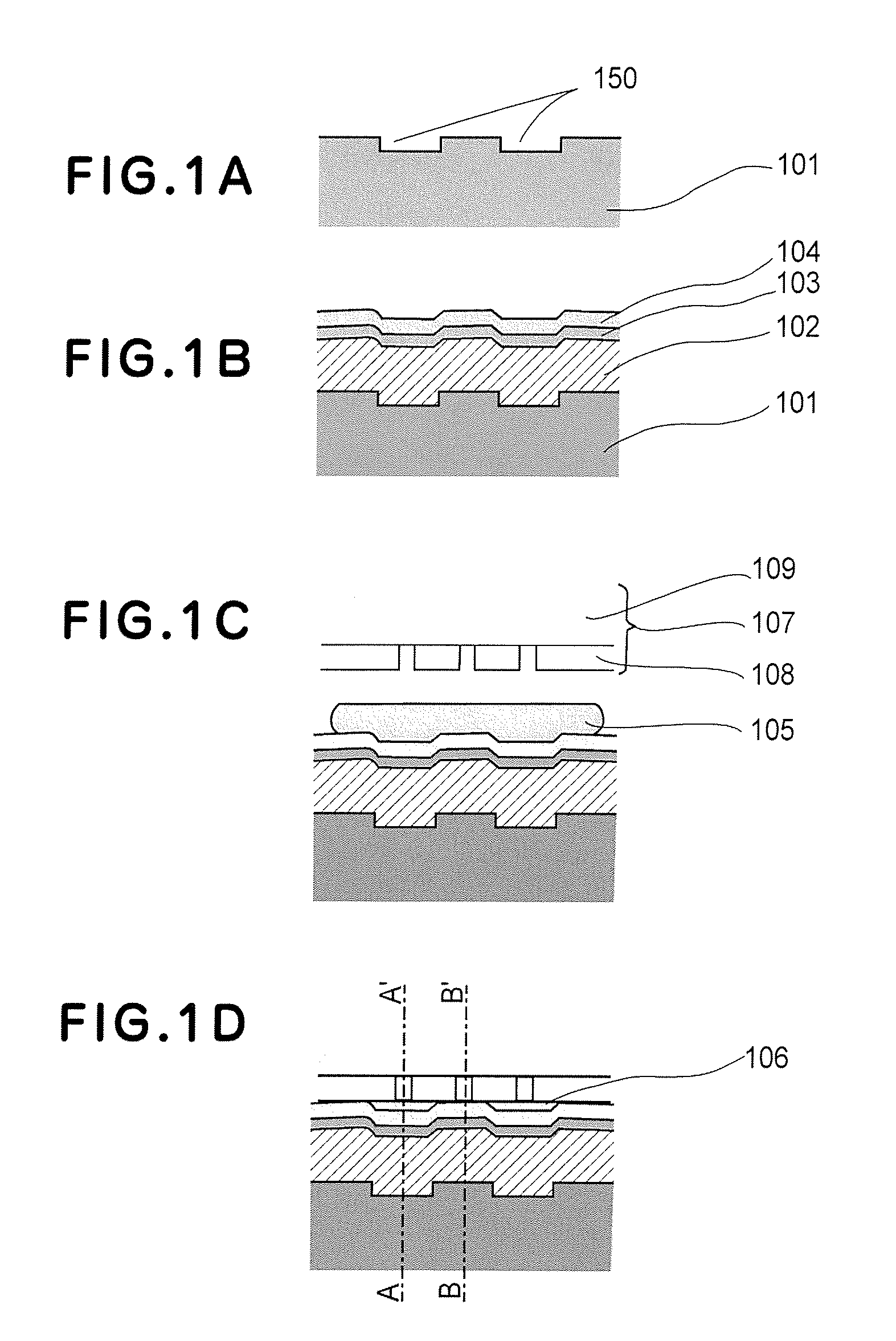
[0011]In accordance with an aspect of the present invention, there is provided a near-field exposure method, comprising: closely contacting an exposure mask having a light blocking film with small openings of a size not greater than a wavelength of exposure light of an exposure light source, to a photoresist layer formed on a substrate having surface unevenness; and projecting the exposure light of the exposure light source onto the exposure mask so that the photoresist is exposed based on near-field light escaping from the small openings, wherein the near-field exposure is carried out while keeping both a contact region in which the light blocking film and the photoresist layer are in contact with each other and a liquid region in which an interspace between the light blocking film and the photoresist layer is filled with a liquid, coexisting between the light blocking film and the photoresist layer.

Problems solved by technology

Although the optical lithography has advanced with respect to the microprocessing resolution, there still remain some problems to be solved to enable microprocessing resolution of less than 0.1 μm; namely, further shortening of the wavelength of a light source and development of lenses usable with such wavelength region, for example.
However, these methods may cause the following inconveniences.
Namely, when a resist film is formed on a non-flat substrate and near-field exposure is performed thereto, the resist film surface may not be completely flat and it causes a difficulty of controlling the unevenness of exposure state.
This makes the device structure quite complicated and causes a decrease of machining precision due to the deformation.

Method used


Image

  • Near-field exposure method
  • Near-field exposure method

Examples


Embodiment Construction

[0017]Preferred embodiments of the present invention will now be described with reference to the attached drawings.

[0018]A near-field exposure method according to an embodiment of the present invention may include closely contacting an exposure mask having a light blocking film with small openings of a size not greater than a wavelength of exposure light of an exposure light source, to a photoresist layer formed on a substrate having surface unevenness, and projecting the exposure light of the exposure light source onto the exposure mask so that the photoresist is exposed based on near-field light escaping from the small openings, wherein the near-field exposure may be carried out while keeping both a contact region in which the light blocking film and the photoresist layer are in contact with each other and a liquid region in which an interspace between the light blocking film and the photoresist layer is filled with a liquid, coexisting between the light blocking film and the phot...


PUM

PropertyMeasurementUnit
heightaaaaaaaaaa
thicknessaaaaaaaaaa
thicknessaaaaaaaaaa

Abstract

A near-field exposure method includes closely contacting an exposure mask having a light blocking film with small openings of a size not greater than a wavelength of exposure light of an exposure light source, to a photoresist layer formed on a substrate having surface unevenness, and projecting the exposure light of the exposure light source onto the exposure mask so that the photoresist is exposed based on near-field light escaping from the small openings, wherein the near-field exposure is carried out while keeping both a contact region in which the light blocking film and the photoresist layer are in contact with each other and a liquid region in which an interspace between the light blocking film and the photoresist layer is filled with a liquid, coexisting between the light blocking film and the photoresist layer, whereby fluctuation of exposure state of the near-field exposure due to surface unevenness of the substrate is reduced effectively.

Description

FIELD OF THE INVENTION AND RELATED ART[0001]This invention relates to a near-field exposure method. More particularly, the invention concerns a near-field exposure method in which a mask for exposure is placed close to a substrate to be exposed and the substrate is exposed by use of near-field light escaping from very small openings formed in the exposure mask.[0002]With increasing capacity of semiconductor memories and increasing speed and density of CPUs, further improvements in the microprocessing technology based on optical lithography have been required as a crucial key.[0003]Generally, optical lithography machines have a microprocessing limit of around the wavelength of a light source. Because of this, shortening of the wavelength has been attempted, such as use of a near-ultraviolet radiation laser for a light source of optical lithography machines, for example. Currently, the microprocessing resolution of around 0.1 μm order has been enabled.[0004]Although the optical lithog...

Claims


Application Information

Patent Timeline
Patent Type & Authority Applications(United States)
IPC IPC(8): G03F7/20
CPCB82Y10/00G03F7/70383G03F7/2014G03F1/14G03F1/50
Inventor MIZUTANI, NATSUHIKOINAO, YASUHISA
Owner CANON KK
Learn More