Antistatic component and method of manufacturing the same

a technology of antistatic components and components, applied in the direction of electrostatic charges, contact mechanisms, coupling device connections, etc., can solve the problems of easy damage to the button surface, easy wear and tear of the button surface exposed to the outside, and easy breakage, so as to prevent the penetration of static electricity, maintain the durability and appearance of the part, and effectively protect the

Active Publication Date: 2007-12-20
LG ELECTRONICS INC
View PDF2 Cites 6 Cited by
  • Summary
  • Abstract
  • Description
  • Claims
  • Application Information

AI Technical Summary

Benefits of technology

[0021]With the antistatic component constructed as above and the method of manufacturing the same according to the present invention, penetration of static electricity is prevented while the durability and appearance of a part is maintained. Thus, there are advantages in that an internal system can be effectively protected and productivity can be improved while the appearance of the part is sufficiently decorated.

Problems solved by technology

Thus, when the user of the electronic device pushes the plated button, an electric charge charged to the human body may be transmitted to the switch through the button, which may cause ESD (Electrostatic Discharge).
If static electricity flows into the system unit through the plated button, it may damage parts or disturb the system unit, thereby causing malfunction.
However, there are problems in that the intermediate member made of an insulating material should be separately prepared and a process of installing and fixing the member should be added.
However, in this case, the button surface exposed to the outside may be worn away or easily broken down.

Method used


Image

  • Antistatic component and method of manufacturing the same
  • Antistatic component and method of manufacturing the same
  • Antistatic component and method of manufacturing the same

Examples


Embodiment Construction

[0028]Hereinafter, preferred embodiments of an antistatic component and a method of manufacturing the same according to the present invention will be described in detail with reference to the accompanying drawings.

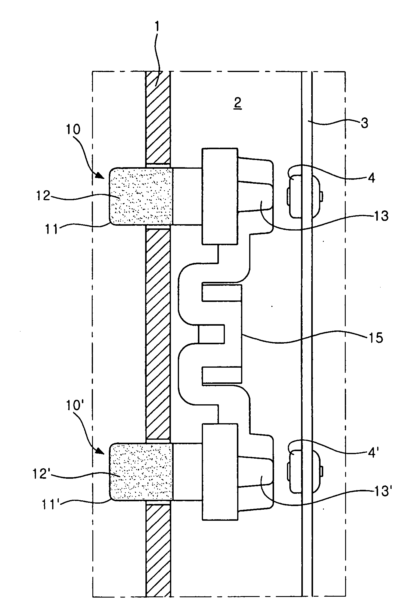
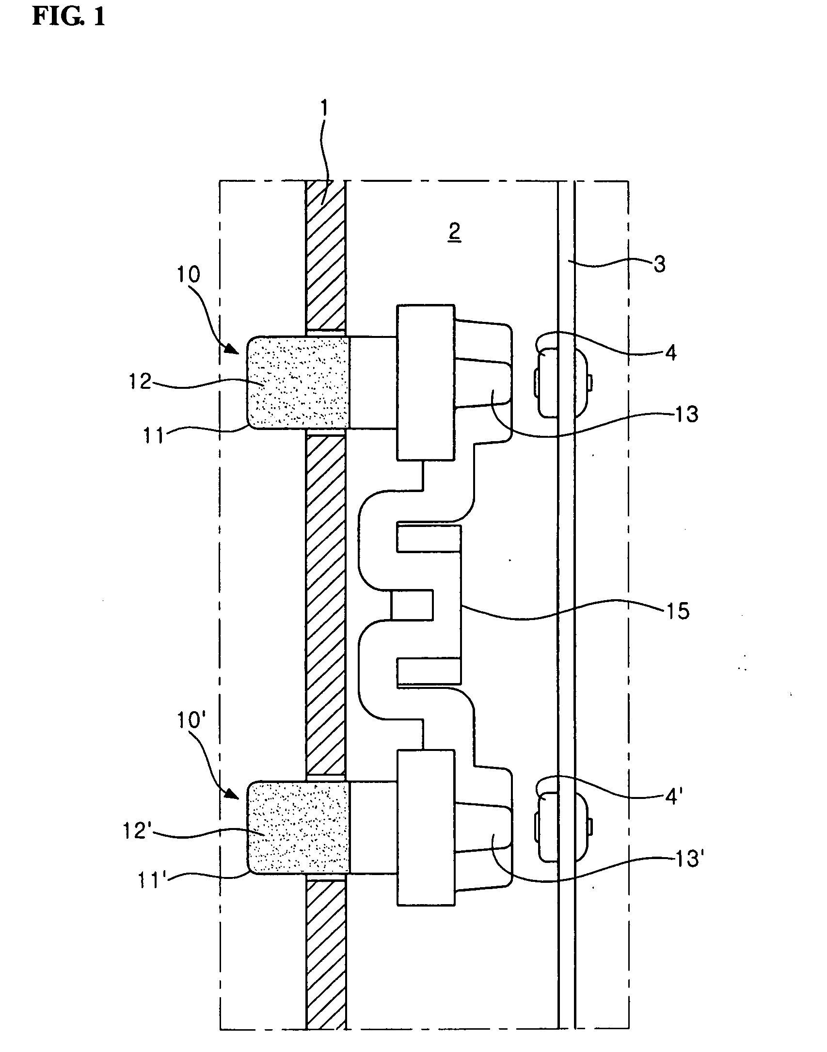
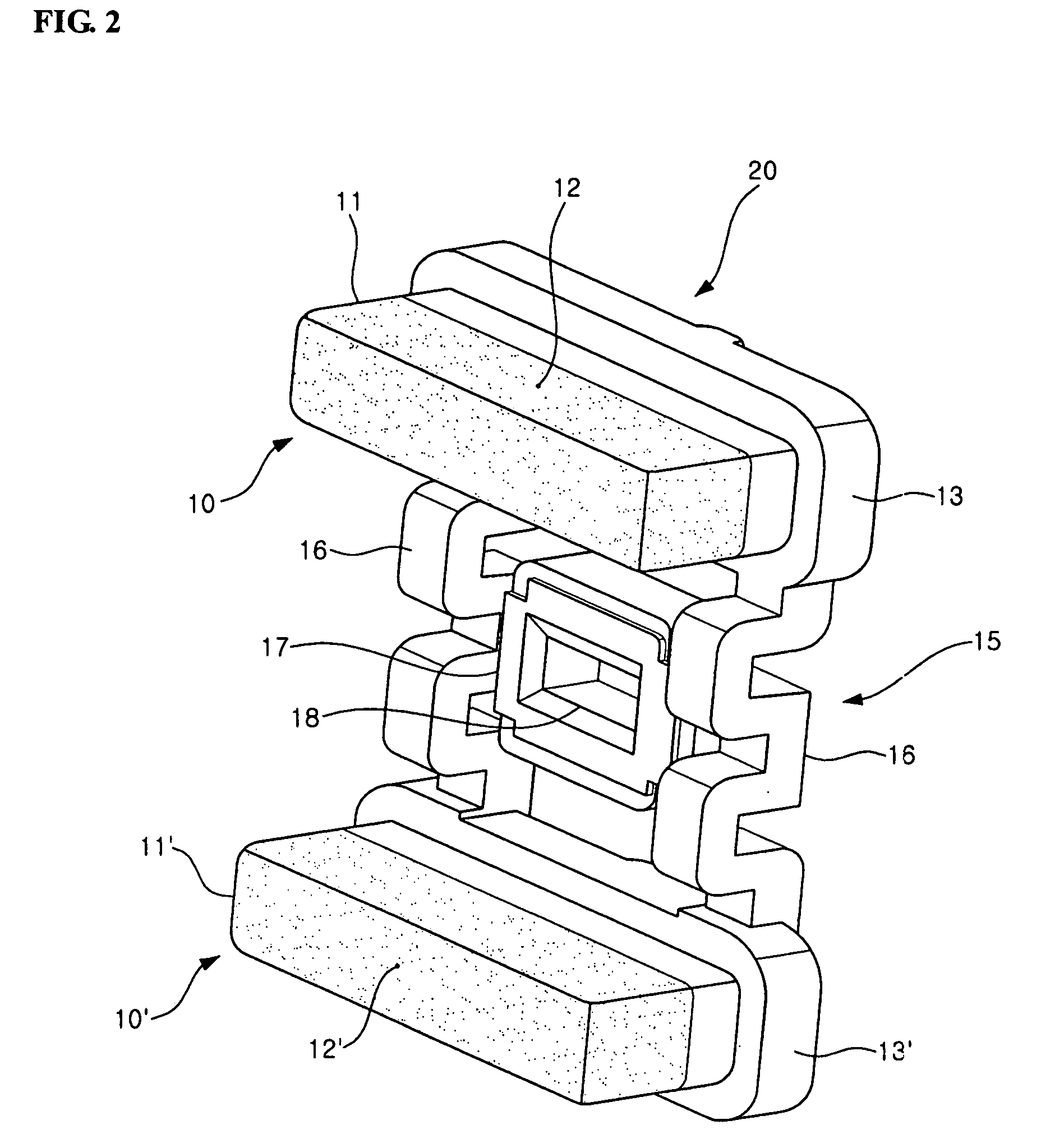
[0029]FIG. 1 is a partial sectional view showing a button array and its peripheral configuration according to an embodiment of the present invention, FIG. 2 is a perspective view showing the button array of FIG. 1, and FIG. 3 is a perspective view showing an appearance of an electronic product in which the button array of FIG. 2 is installed.

[0030]As shown these figures, an electronic product has a case 1 defining an appearance thereof. The case 1 has a certain inner space 2 therein. A board 3 for mounting various parts thereon is provided in the inner space 2. A tack switch 4 for applying a signal to an internal system is provided on the board 3.

[0031]A button array 20 is provided in the inner space 2. In this embodiment, the button array generally includes a plurality of...


PUM


Abstract

The present invention relates to an antistatic component and a method of manufacturing the same. An antistatic component of the present invention comprises buttons each of which includes a push portion 11 or 11′ formed at one end of the button and made of a first resin and a switch contact 13 or 13′ formed at the other end of the button and made of a second resin; and an elastically-deformable connection portion 15 formed integrally with the switch contact 13 or 13′ so as to connect the plurality of buttons to one another. The push portion is exposed outward to be pushed and has a plating layer 12 or 12′ formed thereon, and the switch contact selectively operates a tact switch 4 or 4′. The first resin comprises a plating material and the second resin comprises a non-plating material. The switch contact and the connection portion, and the push portion are formed integrally with each other by means of dual injection molding. With the antistatic component and the method of manufacturing the same according to the present invention constructed as above, penetration of static electricity is prevented while the durability and appearance of the button are maintained. Thus, there are advantages in that the appearance of a part can be sufficiently decorated, an internal system can be effectively protected, and a process of manufacturing a part can be simplified, resulting in improved productivity.

Description

BACKGROUND OF THE INVENTION[0001]1. Field of the Invention[0002]The present invention relates to an antistatic component and a method of manufacturing the same, and more particularly, to an antistatic component for preventing introduction of static electricity into an internal system and a method of manufacturing the component.[0003]2. Description of the Related Art[0004]Generally, an electronic product includes a system unit in which various parts are mounted to a circuit board to execute operations of the electronic product. A variety of parts are electrically connected to the system unit. Among these parts, some parts are charged with static electricity in certain cases. Typical examples of these parts are a button and a connector. Hereinafter, the related art will be described in connection with a button.[0005]A potable electronic device such as a cellular phone or PDA is provided with a button array for use in selectively manipulating switches provided on a circuit board within...

Claims


Application Information

Patent Timeline
Patent Type & Authority Applications(United States)
IPC IPC(8): H01H13/14
CPCH01H13/70H01H13/88H01H2221/044H01H2221/054H01H2221/074H01R13/6599H01H2233/004H01H2233/03H01H2239/008H01R13/6485H01H2229/046H05F1/00
Inventor KIM, JAE MOON
Owner LG ELECTRONICS INC
Why Eureka
Try Eureka