Arrangements of color pixels for full color OLED

a color pixel and display device technology, applied in the direction of discharge tube luminescnet screens, discharge tube/lamp details, electric discharge lamps, etc., can solve the problems of mixing colors or non-emission of light, a considerable level of difficulty in the display panel manufacturing process, and a large amount of difficulty in the manufacturing process of display panels

Inactive Publication Date: 2008-01-03
AU OPTRONICS CORP
View PDF21 Cites 268 Cited by
  • Summary
  • Abstract
  • Description
  • Claims
  • Application Information

AI Technical Summary

Problems solved by technology

Such an arrangement of the sub-pixel devices may pose a considerable level of difficulty in the display panel manufacturing process.
This may cause misalignment of the sub-pixel devices in the OLED display panels.
An example of the sub-pixel device misalignment is shown in FIG. 6b. Misalignment in the sub-pixel devices results in problems such as no deposition of the organic layer and thus the short-circuiting of the lower electrode and the upper electrode of the sub-pixel device, and deposition of the organic layer in an adjacent sub-pixel, which causes mixing of colors or non-emission of light.
The arrangement of the sub-pixel devices also makes fabricating a shadow mask very difficult.
In addition, it is hard to manufacture a high-resolution OLED display using the arrangement of the sub-pixel devices.
Therefore, a heretofore unaddressed need exists in the art to address the aforementioned deficiencies and inadequacies.

Method used


Image

  • Arrangements of color pixels for full color OLED
  • Arrangements of color pixels for full color OLED
  • Arrangements of color pixels for full color OLED

Examples


Embodiment Construction

[0025]The present invention is more particularly described in the following examples that are intended as illustrative only since numerous modifications and variations therein will be apparent to those skilled in the art. Various embodiments of the invention are now described in detail. Referring to the drawings, like numbers indicate like components throughout the views. As used in the description herein and throughout the claims that follow, the meaning of “a”, “an”, and “the” includes plural reference unless the context clearly dictates otherwise. Also, as used in the description herein and throughout the claims that follow, the meaning of “in” includes “in” and “on” unless the context clearly dictates otherwise.

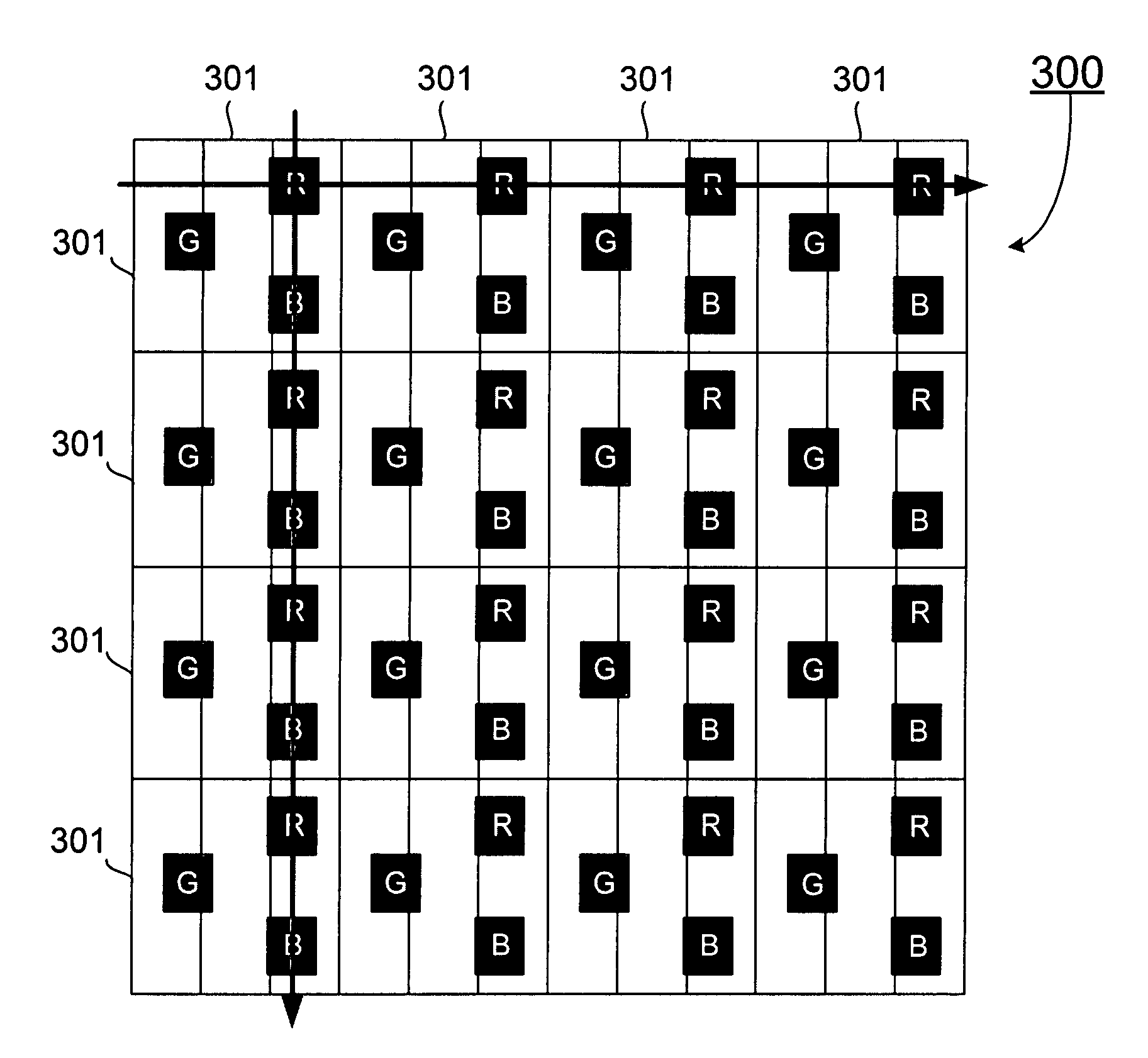
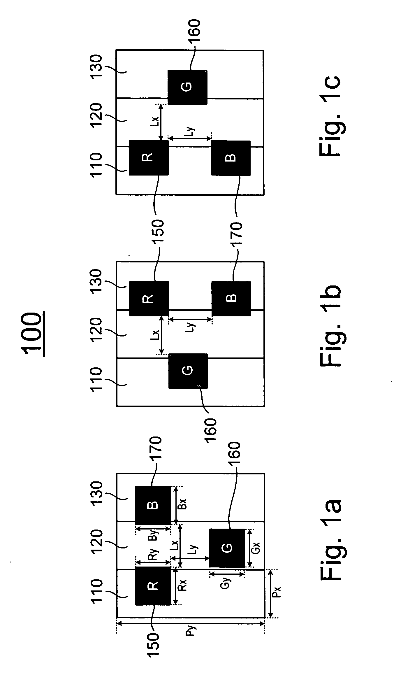
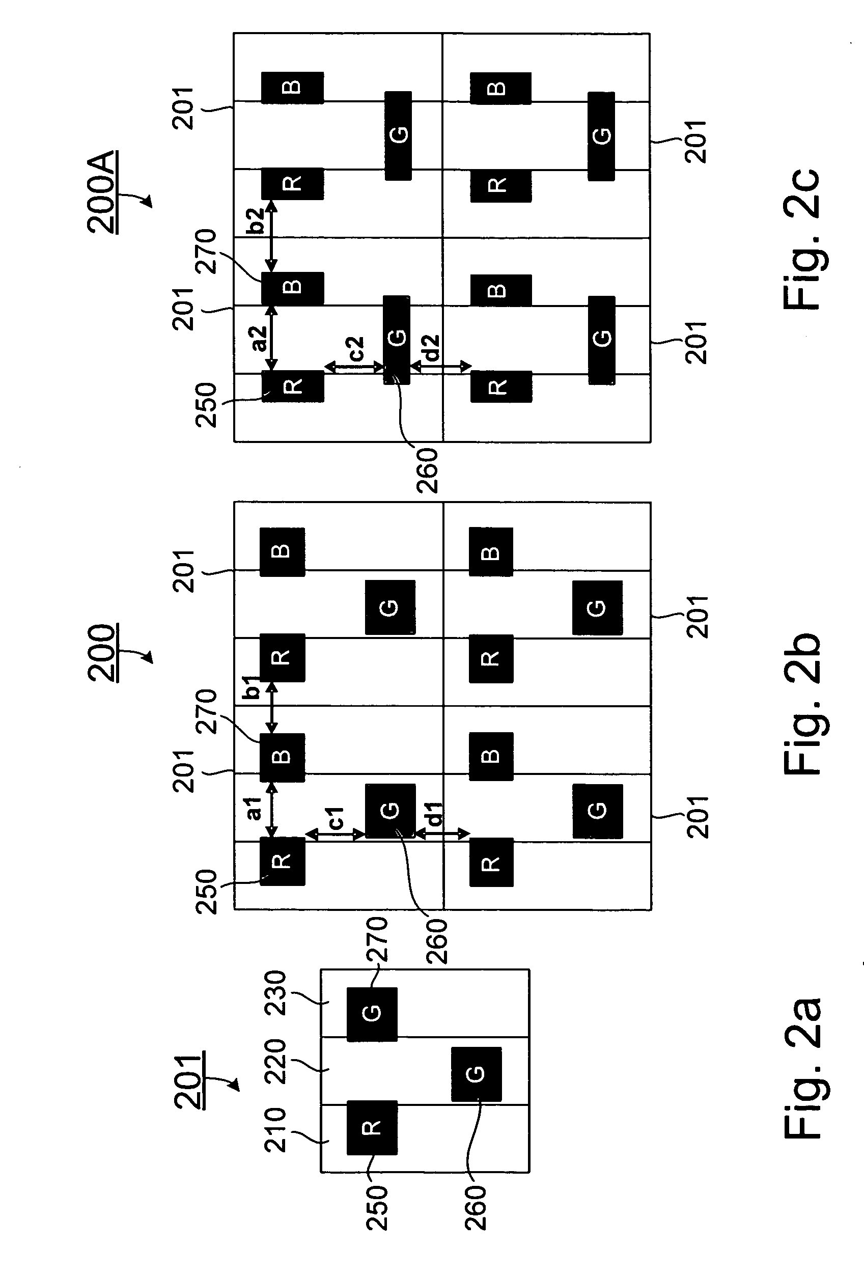
[0026]The description will be made as to the embodiments of the present invention in conjunction with the accompanying drawings in FIGS. 1-5. In accordance with the purposes of this invention, as embodied and broadly described herein, this invention, in one aspect, relate...


PUM


Abstract

A color display panel formed with a plurality of pixels in a matrix with a row direction and a column direction, wherein each pixel comprises a first sub-pixel, a second sub-pixel and a third sub-pixel adjacently aligned along the row direction of the pixel matrix, and a red light emission zone, a green light emission zone and a blue light emission zone. In one embodiment, the color display panel comprises an arrangement of the red, green and blue light emission zones of a pixel in a triangle with the geometrical center of each emission zone located at a respective vertex of the triangle such that one side of the triangle is substantially parallel to one of the row direction and the column direction, thereby in the plurality of pixels, any two adjacent light emission zones of different colors in the row direction define a gap having a distance, and any two adjacent light emission zones of different colors in the column direction define a gap having a distance that is substantially or nearly the same as the distance of the gap defined between two adjacent light emission zones of different colors in the row direction.

Description

FIELD OF THE INVENTION[0001]The present invention relates generally to a full color display, and more particularly, to an organic light emitting diode display device with arrangements of sub-pixels.BACKGROUND OF THE INVENTION[0002]Generally, a full color display panel is composed of red, green and blue sub-pixel devices, arranged in a stripe form, a mosaic form or a delta form, so as to provide full color effects by mixing the light of these colors emitted from the individual sub-pixel devices in the display panel. Due to its compact size, high resolution, low power consumption, self-emission and fast response, organic light emitting diode (OLED) display panels have widespreadly been used for high definition displays of full color images.[0003]Conventionally, an arrangement of the red, green and blue sub-pixel devices of liquid crystal displays is employed for OLED display panels, which is shown in FIGS. 6a and 6b. In this arrangement, each pixel 601 in the pixel matrix 600 has a fi...

Claims


Application Information

Patent Timeline
Patent Type & Authority Applications(United States)
IPC IPC(8): H05B33/00H01L51/50
CPCH01L27/3218H01L27/3211H10K59/352H10K59/353
Inventor CHAO, CHING-IANWU, YUAN-CHUN
Owner AU OPTRONICS CORP
Why Eureka
Try Eureka