Supercharge Your Innovation With Domain-Expert AI Agents!

Defect detection system, defect detection method, and defect detection program

a defect detection and defect technology, applied in the field of defect detection systems and defect detection methods, can solve problems such as clustering defects in semiconductor device manufacturing, lowering yield, and general difficulty in detecting the cause of defects

Inactive Publication Date: 2008-01-03
KK TOSHIBA
View PDF5 Cites 35 Cited by
  • Summary
  • Abstract
  • Description
  • Claims
  • Application Information

AI Technical Summary

Benefits of technology

[0019] acquiring information on defect distribution in an area with a size smaller than a size of each of

Problems solved by technology

Thus, it is generally very difficult to detect that the cause of a defect that occurred in the LSI once.
Most of the time, the occurrence of the clustering defect arises from systematic causes resulting from process, manufacturing device and the like, which is a great cause in lowering of yield.
The defect resulting from process, manufacturing device and the like produces a defect pattern inherent in the process or the manufacturing device on the wafer surface.
However, the clustering defect in manufacturing of the semiconductor device does not only appear as a pattern in the wafer surface.
The state of the processing process differs between the central part and the peripheral part of the memory cell array in memory products, and thus defects occur in the state deflected towards the peripheral part of the memory cell array, in which case, the pattern of the clustering defect is produced in the chip partition.
However, when the wafer test result indicating the defects in units of partition with a size larger than or equal to the size of the chip partition is used, pattern classification of the clustering defect and defect detection in the shot partition or the chip partition cannot be performed, and the cause of defect of the semiconductor device cannot be detected at high precision.

Method used


Image

  • Defect detection system, defect detection method, and defect detection program
  • Defect detection system, defect detection method, and defect detection program
  • Defect detection system, defect detection method, and defect detection program

Examples


Embodiment Construction

[0058] The embodiments of the present invention will now be described with reference to the following drawings. Same or similar reference characters are denoted for same or similar components throughout the description of the drawings.

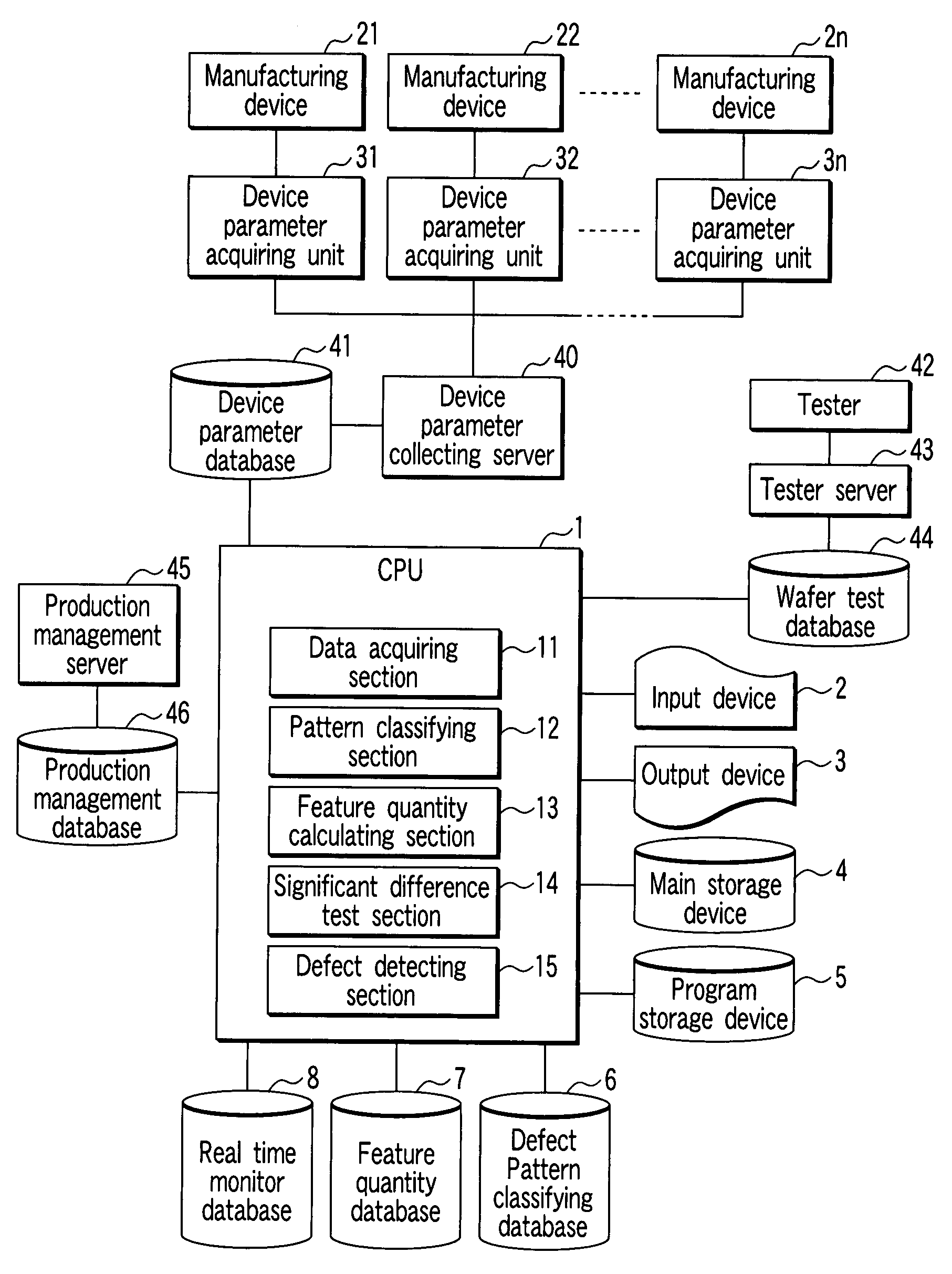
[0059] A defect detection system according to the present embodiment includes a central processing unit (CPU) 1, a device parameter database 41, a production management database 46, a wafer test database 44, a defect pattern classification database 6, a feature quantity database 7, and a real time monitor database 8, which are connected to the CPU 1, as shown in FIG. 1.

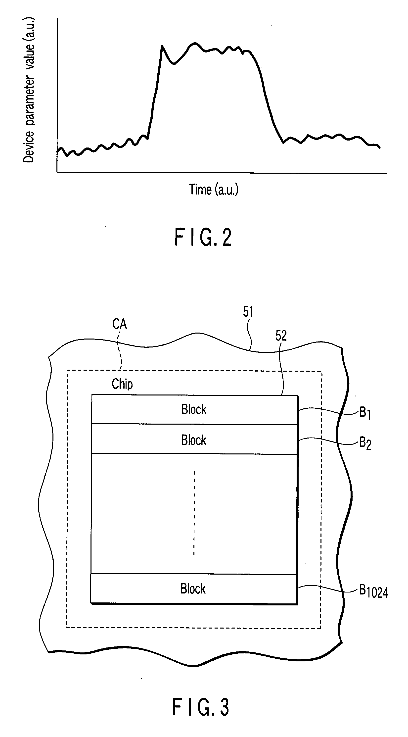
[0060] The CPU 1 includes a data acquiring section 11 that acquires the time series data of device parameters for each of a plurality of manufacturing devices 21, 22, . . . , 2n including an exposure device and information on defect distribution in an area with a size smaller than the size of each of a plurality of chip areas arrayed on the wafer to be processed in each of the pluralit...


PUM


Abstract

A defect detection system includes a data acquiring section that acquires time series data of device parameter of each manufacturing device including an exposure device, and information on defect distribution in an area with a size smaller than a chip area size, a pattern classifying section that assembles the information on the defect distribution in units of shot or chip areas, and classifies the distributions to a defect pattern, a feature quantity calculating section that processes the time series data and calculates a feature quantity, a significant difference test section that calculates occurrence frequency distributions of the shot or chip area wherein the defect pattern to the feature quantity exists and does not exist, respectively, and determines the presence / absence of significant difference between the frequency distributions, and a defect detecting section that detects the device parameter corresponding to the feature quantity as the cause of defect of the defect pattern.

Description

CROSS-REFERENCE TO RELATED APPLICATIONS [0001] This application is based upon and claims the benefit of priority from prior Japanese Patent Application No. 2006-170677, filed Jun. 20, 2006, the entire contents of which are incorporated herein by reference. BACKGROUND OF THE INVENTION [0002] 1. Field of the Invention [0003] The present invention relates to manufacturing of a semiconductor device, in particular, to a defect detection system, a defect detection method, and a defect detection program for detecting the cause of a defect of the semiconductor device. [0004] 2. Description of the Related Art [0005] One of the problems to be addressed in enhancing the productivity of the semiconductor device such as a large-scale integration (LSI) circuit is to enhance the yield. It is important to analyze the yield loss, and ascertain and improve the process, manufacturing device, or design conditions that lead to the cause of yield loss at an early stage in order to enhance the yield. Howe...

Claims


Application Information

Patent Timeline
IPC IPC(8): G06F19/00G01R31/26H01L21/02H01L21/66
CPCG01N21/9501G05B2219/32222G05B2219/32221G05B19/41875Y02P90/02
Inventor MATSUSHITA, HIROSHIARAKAWA, YASUTAKASUGAMOTO, JUNJI
Owner KK TOSHIBA
Features
  • R&D
  • Intellectual Property
  • Life Sciences
  • Materials
  • Tech Scout
  • Unparalleled Data Quality
  • Higher Quality Content
  • 60% Fewer Hallucinations
Learn More