System and method of attenuating electromagnetic interference with a grounded top film

a top film and electromagnetic interference technology, applied in the field of shielding plastic encapsulated circuits from electromagnetic interference, can solve the problems of inability to achieve and inability to use past processes, and achieve the effect of low cost and easy and cost-effective methods

Inactive Publication Date: 2008-01-17
TEXAS INSTR INC
View PDF5 Cites 85 Cited by
  • Summary
  • Abstract
  • Description
  • Claims
  • Application Information

AI Technical Summary

Benefits of technology

[0004]Many electronic integrated circuits are encapsulated in plastic. A standard overmolded process uses a single molded cavity with a number of integrated circuits being encapsulated in the same cavity, and then uses a sawing process (package singulation) for dividing the single molded unit into multiple packages. However it is not possible as

Problems solved by technology

However it is not possible as part of this regular package processing to use a thin metal layer to protect the package from EMI due to the fact that the metal layer needs to

Method used


Image

  • System and method of attenuating electromagnetic interference with a grounded top film
  • System and method of attenuating electromagnetic interference with a grounded top film
  • System and method of attenuating electromagnetic interference with a grounded top film

Examples


Embodiment Construction

[0020]While the making and using of various embodiments of the present invention are discussed in detail below, it should be appreciated that the present invention provides many applicable inventive concepts that can be embodied in a wide variety of specific contexts. The specific embodiments discussed herein are merely illustrative of specific ways to make and use the invention and do not delimit the scope of the invention.

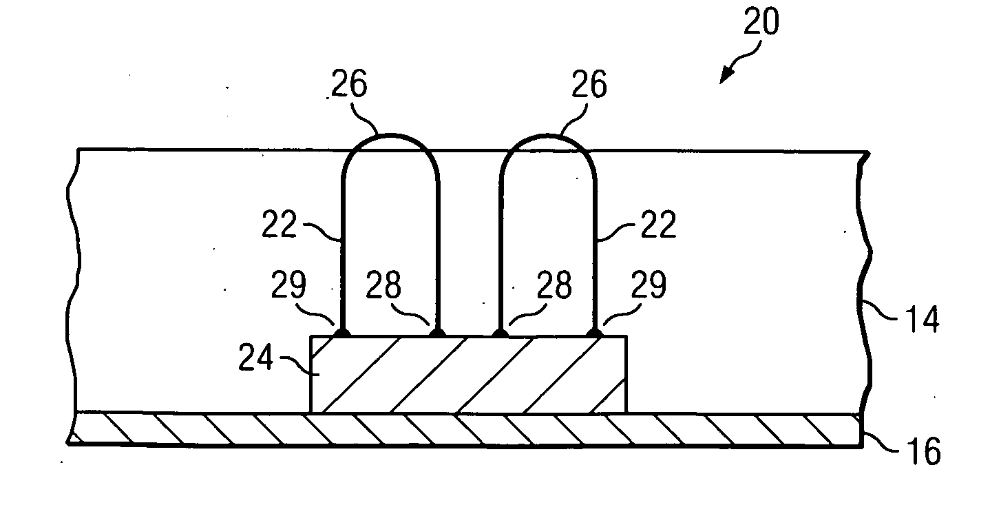
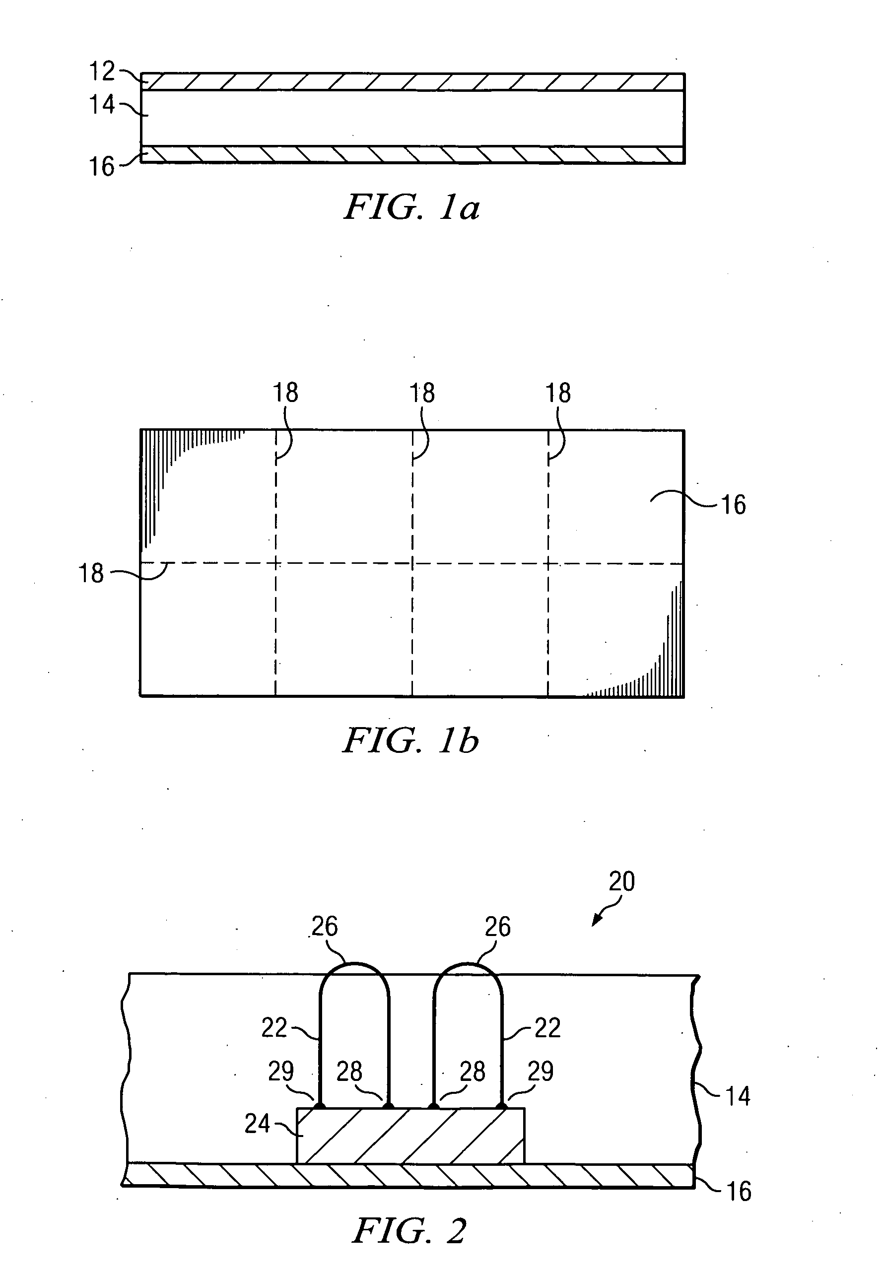
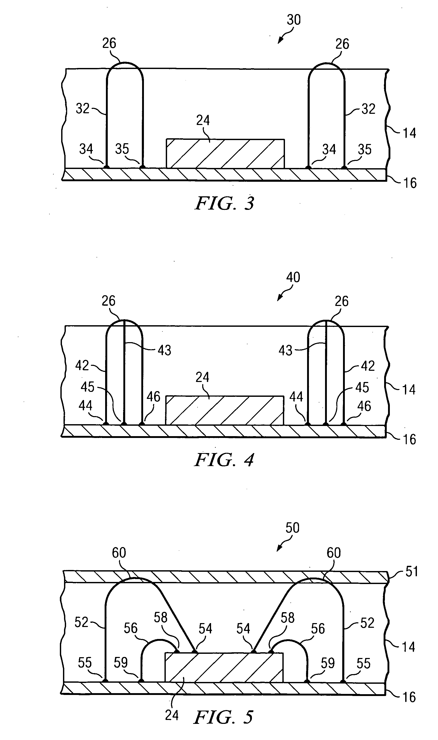
[0021]In one embodiment, the present invention solves the problem of creating a connection to the metal layer over the mold material by using a grounded wirebond (with a package-high loop) from the die / substrate to the top of the mold cap (and, e.g. back to the die / substrate connected to the ground bus on the die / substrate). After the molding is completed, the wire loops that have been added are exposed at the surface of the mold cap for all the packages prior to saw singulation. This exposure can be further enhanced by a dry etch process to guarantee a good elec...


PUM


Abstract

A plastic integrated circuit package often includes one or more integrated circuit elements that are sensitive to outside electromagnetic fields and also may generate electromagnetic fields that may interfere with other circuits outside of the package. The package herein has a top metal film to attenuate such electromagnetic fields, using a wire loop extending through the encapsulating compound to the metal film on top of encapsulating compound to provide electrical connection between top EMI film and end-and-ground junctions at grounds on die or on end-and-ground junctions at grounds on substrate.

Description

FIELD OF THE INVENTION[0001]The present invention relates generally to the field of electronic circuits and, more particularly, to shielding plastic encapsulated circuits from electromagnetic interference.BACKGROUND OF THE INVENTION[0002]Electrical devices generally emit electrical fields, magnetic fields, or a combination of both (electromagnetic fields). For example, an integrated circuit structure (e.g., an integrated circuit chip) within an electrical device may emit one or more electrical fields, magnetic fields, or electromagnetic fields, which may result in the electrical device emitting such one or more fields. An electromagnetic field emitted from one electrical device may interfere with another electrical device. This interference may be referred to as electromagnetic interference (EMI). As an example, electrical devices may emit radio frequency (RF) signals, microwave signals, or other electromagnetic signals, which may interfere with other electrical devices.[0003]Additi...

Claims


Application Information

Patent Timeline
IPC IPC(8): H01L21/00
CPCH01L21/565H01L23/552H01L2224/16225H01L2924/12041H01L2224/97H01L2924/01033H01L2924/01006H01L2924/00014H01L2924/3025H01L2924/19107H01L2924/14H01L2924/01079H01L2924/01078H01L2924/01057H01L24/45H01L24/48H01L24/49H01L24/85H01L24/97H01L2224/45144H01L2224/48091H01L2224/4813H01L2224/48464H01L2224/48599H01L2224/4917H01L2224/85H01L2924/01005H01L2924/01013H01L2924/01029H01L2224/78H01L2924/00H01L2224/81H01L2924/181H01L2224/85399H01L2224/05599
Inventor HOWARD, GREGORY ERICGUPTA, VIKASSIBIDO, WILMAR
Owner TEXAS INSTR INC
Why Eureka
Try Eureka