Array substrate, display device having the same and method of manufacturing the same

a display device and substrate technology, applied in the direction of identification means, instruments, optics, etc., can solve the problems of deterioration of image display quality, deterioration of etching profile of lines, and deterioration of uniformity of metal layers, so as to reduce line resistance and the effect of occurrence of line defects

Inactive Publication Date: 2008-01-24
SAMSUNG DISPLAY CO LTD
View PDF4 Cites 38 Cited by
  • Summary
  • Abstract
  • Description
  • Claims
  • Application Information

AI Technical Summary

Benefits of technology

[0007] The present invention provides an array substrate capable of decreasing line resistance and the occurrence of line defects.

Problems solved by technology

Therefore, the image display quality is deteriorated.
Furthermore, when a metal layer is etched to form the lines, the etching uniformity of the metal layer may be deteriorated, which may deteriorate the etching profile of the lines.

Method used


Image

  • Array substrate, display device having the same and method of manufacturing the same
  • Array substrate, display device having the same and method of manufacturing the same
  • Array substrate, display device having the same and method of manufacturing the same

Examples


example i

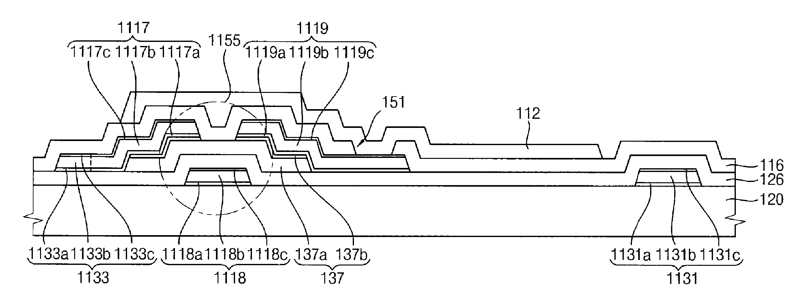
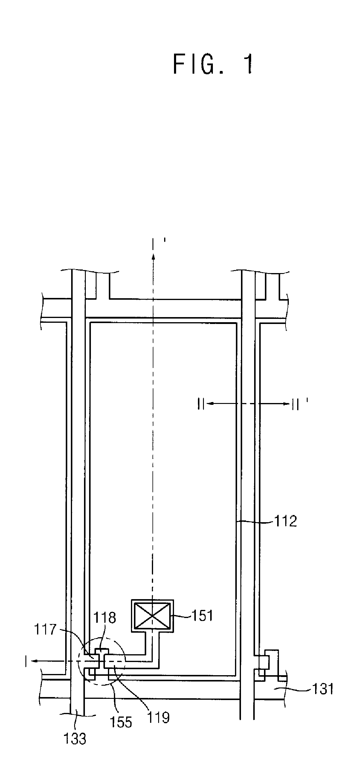
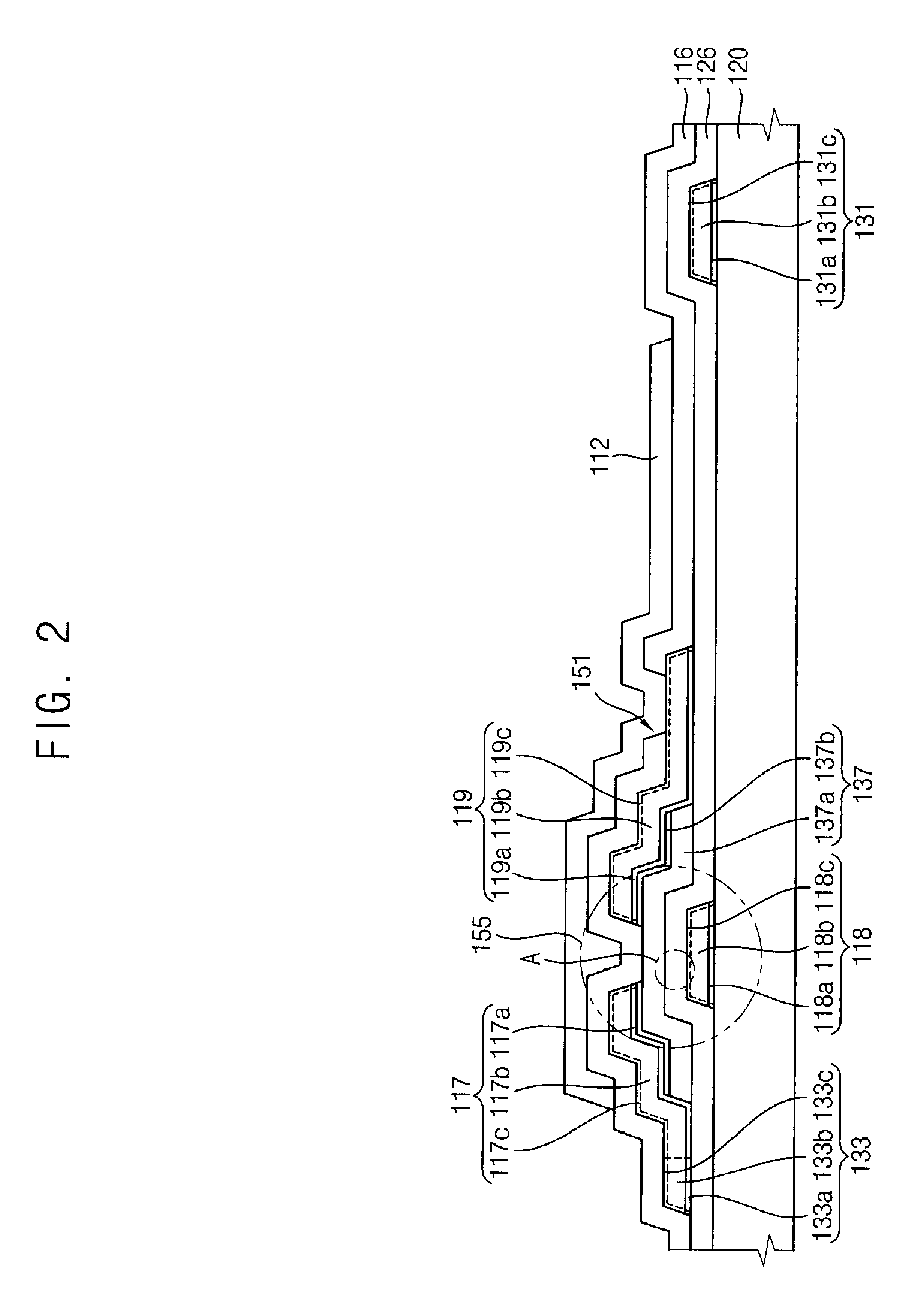
[0118] A primary gate conductive pattern 188d (shown in FIG. 8) was treated by nitride plasma or hydrogen plasma. A gate insulating layer having a multilayered structure and including a low density silicon nitride layer and a high density silicon nitride layer was deposited on the substrate. The nitride plasma or the hydrogen plasma was generated by an electric power of about 600W during about 20 seconds. An electric power of about 900W was applied to a gas mixture including silane gas and a nitride mixture gas and the amount of silane gas in the gas mixture was about 2.24% by volume. An electric power of about 1200W was applied to a gas mixture including silane gas and a nitride mixture gas and the amount of the silane gas in the gas mixture was about 6.43% by volume.

[0119] When a first low density silicon nitride layer, a high density silicon nitride layer, and a second low density silicon nitride layer were formed after the nitride plasma treatment, the resistance of the gate li...


PUM

PropertyMeasurementUnit
electric poweraaaaaaaaaa

Abstract

An array substrate includes a switching element, a signal transmission line, a passivation layer and a pixel electrode. The switching element is disposed on an insulating substrate. The signal transmission line is connected to the switching element and includes a barrier layer, a conductive line, and a copper nitride layer. The barrier layer is disposed on the insulating substrate. The conductive line is disposed on the barrier layer and includes copper or copper alloy. The copper nitride layer covers the conductive line. The passivation layer covers the switching element and the signal transmission line and has a contact hole through which a drain electrode of the switching element is partially exposed. The pixel electrode is disposed on the insulating substrate, and is connected to the drain electrode of the switching element through the contact hole.

Description

CROSS-REFERENCE TO RELATED APPLICATIONS [0001] The present application claims priority from and the benefit of Korean Patent Application No. 2006-67979, filed on Jul. 20, 2006, the disclosure of which is hereby incorporated by reference for all purposes as if fully set forth herein. BACKGROUND OF THE INVENTION Field of the Invention [0002] The present invention relates to an array substrate, a display device including the array substrate, and a method of manufacturing the array substrate. More particularly, the present invention relates to an array substrate capable of decreasing line resistance and the occurrence of line defects, a display device including the array substrate, and a simplified method of manufacturing the array substrate. DISCUSSION OF THE BACKGROUND [0003] An array substrate of a flat panel display device includes various lines for transmitting signals, which are formed through thin film deposition processes. [0004] In the flat panel display device, the length of t...

Claims


Application Information

Patent Timeline
Patent Type & Authority Applications(United States)
IPC IPC(8): H01L29/04H01L21/00G02F1/1362G09F9/30H01L21/28H01L21/318H01L21/3205H01L21/336H01L21/768H01L23/532H01L29/417H01L29/423H01L29/49H01L29/786
CPCG02F1/136286H01L27/124G02F2001/136295G02F2001/13629G02F1/13629G02F1/136295H01L27/1214H01L29/458H01L29/4908
Inventor LEE, JE-HUNKIM, DO-HYUNLEE, EUN-GUKJEONG, CHANG-OH
Owner SAMSUNG DISPLAY CO LTD
Why Eureka
Try Eureka