Semiconductor device

a technology of semiconductor devices and semiconductor chips, applied in the field of information recording carriers, can solve problems such as easy breakage of ic tags, and achieve the effects of preventing defective operation of a semiconductor chip due to stress on the semiconductor chip, enhancing the rigidity of a semiconductor device, and maintaining durability and desired functions of the semiconductor devi

Inactive Publication Date: 2008-01-31
SEMICON ENERGY LAB CO LTD
View PDF19 Cites 22 Cited by
  • Summary
  • Abstract
  • Description
  • Claims
  • Application Information

AI Technical Summary

Benefits of technology

[0016]In accordance with the present invention, rigidity of a semiconductor device can be enhanced by forming a body structure with ceramic or the like for protecting a semiconductor chip, so that durability and desired function of the semiconductor device can be maintained. For example, even when pressure is applied by a pointed object such as a pen tip, defective operation of a semiconductor chip due to stress to the semiconductor chip can be prevented. Further, the semiconductor chip can tolerate a bending stress.
[0017]In the body structure formed of ceramic or the like, a connection portion between an antenna and an integrated circuit is formed, and thus the integrated circuit part can be connected to the antenna without thickening the semiconductor device. Since the body structure is formed of an elastic material such as ceramic, defective connection with the antenna caused by bending stress can be prevented.
[0018]A portion of passive parts constituting a functional circuit is formed in the body structure, thereby miniaturizing the semiconductor chip. Further, a memory can be expanded in a spare region. Additionally, other functional circuits can be provided in such a spare region as well. Thus, the semiconductor device can be multifunctional and highly-functional.

Problems solved by technology

However, there arises a problem in that an IC tag is easily broken by pressure applied by a pointed object or bending stress, as the IC tag becomes thinner.

Method used


Image

  • Semiconductor device
  • Semiconductor device
  • Semiconductor device

Examples


embodiment mode 1

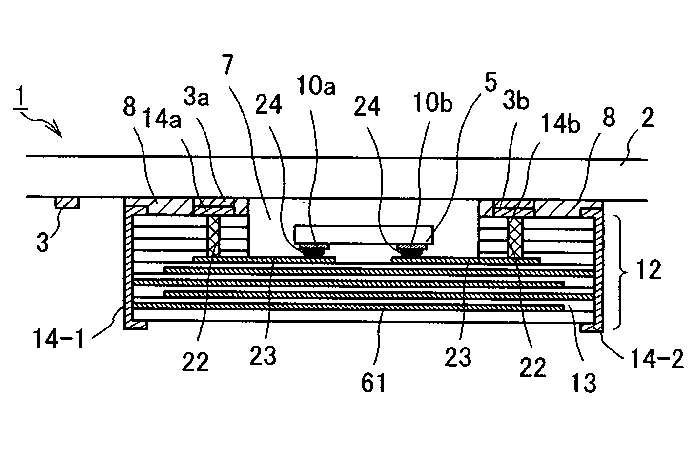
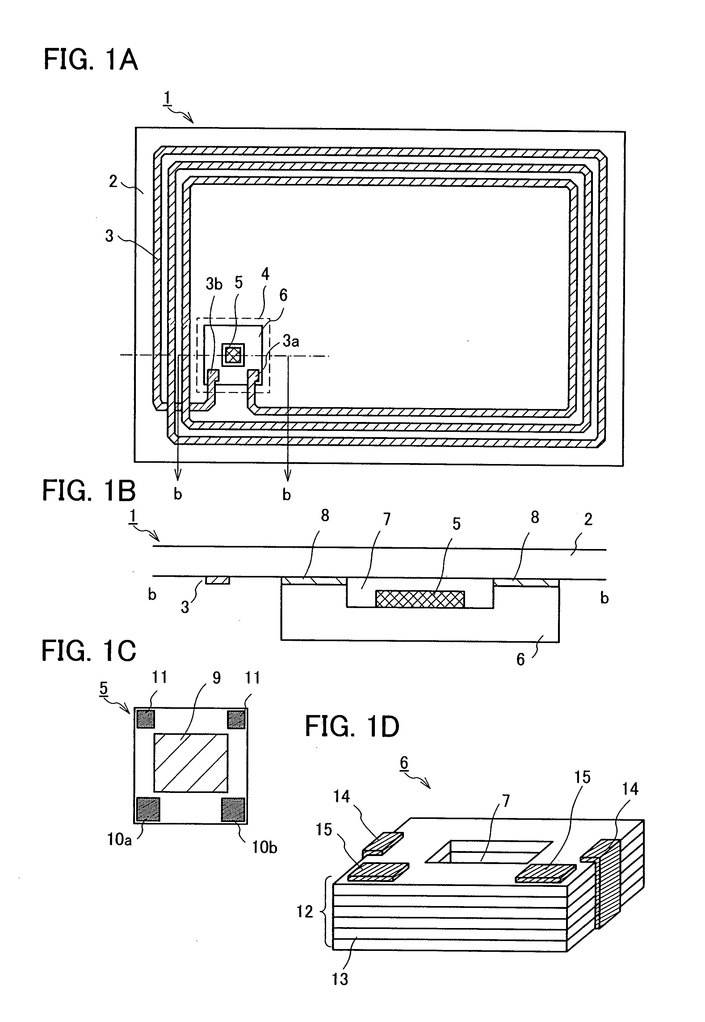
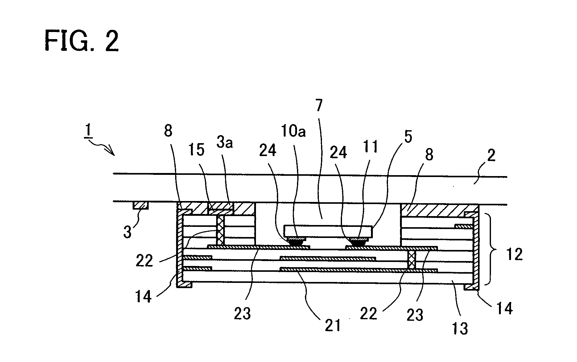
[0030]Embodiment Mode 1 will describe a semiconductor device of the present invention with reference to FIGS. 1A to 1D. FIGS. 1A to 1D illustrate a mode in which a semiconductor device of the present invention is used as an inlet incorporated in a plastic card or an inlet embedded in paper. FIG. 1A is a plan view of an inlet 1, and FIG. 1B is a cross-sectional view taken along the dotted line b-b of FIG. 1A.

[0031]The inlet 1 includes an antenna 3 formed on a base material 2 and an integrated circuit part 4 connected to the antenna 3. The integrated circuit part 4 includes a semiconductor chip 5 and a body structure 6, and the semiconductor chip 5 is fixed on the bottom of a concave portion 7 formed in the body structure 6. The body structure 6 is fixed on the base material by a fixing agent 8 such as a resin. By this configuration, the integrated circuit part 4 is fixed on the base material 2. As for the antenna 3, an insulating layer is formed in an overlapping portion of wirings i...

embodiment mode 2

[0056]A part of a passive element constituting an integrated circuit part 4 can be formed in a body structure 6. For reducing the power consumption, the passive element formed in the body structure 6 is preferably an element which does not need power generated by a power source circuit 42. For example, a part of or the whole capacitor constituting a detecting capacitor portion 44 can be provided in the body structure 6. In addition, a part of or the whole capacitor constituting a storage capacitor portion 48 which serves as a power source supplier can be provided in the body structure 6.

[0057]In this embodiment mode, a mode in which a capacitor is formed in the body structure 6 will be described with reference to FIGS. 5A and 5B. FIGS. 5A and 5B are cross-sectional views of an inlet 1. FIG. 5A is a cross-sectional view illustrating connection between the semiconductor chip 5 and the passive element, and FIG. 5B is a cross-sectional view illustrating connection between the semiconduc...

embodiment mode 3

[0063]In a body structure 6 (multilayer substrate 12), internal wiring layers 21 are formed into predetermined patterns, and stacked. The internal wiring layers 21 are connected to each other by a penetration electrode to form a loop antenna, or a coil antenna. Embodiment Mode 3 will describe a mode in which a second antenna is formed in the body structure 6.

[0064]First, a circuit configuration of an inlet 1 in Embodiment Mode 3 will now be described as an example. FIG. 6 is a block circuit diagram of the inlet 1. A power-feeding antenna 70 (a second antenna) is provided in an integrated circuit part 4. A detecting capacitor 44a for a power source circuit of a detecting capacitor portion 44 is connected to the power-feeding antenna 70, not to the antenna 3 (a first antenna). The other configurations are similar to those of the block circuit diagram shown in FIG. 4.

[0065]In this embodiment mode, the power-feeding antenna 70 provided in the integrated circuit part 4 is formed in the m...


PUM


Abstract

In inlets used for ID tags and the like, a defective connection between an integrated circuit part and an antenna is suppressed by improvement of tolerance for a bending or a pressing pressure. The integrated circuit part includes a semiconductor chip and a multilayer substrate having a concave portion. The semiconductor chip is mounted on the bottom of the concave portion. The multilayer substrate includes a connection electrode at the top surface and a connection electrode connected to the semiconductor chip on the bottom of the concave portion. The connection electrode on the bottom of the concave portion is connected to the connection electrode at the top surface by a penetration electrode inside a multilayer substrate. By such a configuration, the semiconductor chip is connected to the antenna.

Description

BACKGROUND OF THE INVENTION[0001]1. Field of the Invention[0002]The present invention relates to information recording carriers which are utilized in the information technology referred to as RFID (Radio Frequency Identification). Specifically, the present invention relates to semiconductor devices capable of inputting and outputting information by electromagnetic waves. Moreover, the present invention relates to semiconductor devices such as noncontact type IC tags or inlets (also referred to as inlays and inserts) incorporated in such noncontact type IC tags.[0003]2. Description of the Related Art[0004]Information technology which is referred to as RFID (Radio Frequency Identification) has been spreading. For example, an IC tag is known, which is a tag having an outside dimension of several centimeters, storing data and communicating with a reader wirelessly. An IC tag includes an antenna and an IC chip having a communication circuit and a memory.[0005]One mode of an IC tag is kno...

Claims


Application Information

Patent Timeline
Patent Type & Authority Applications(United States)
IPC IPC(8): H01L23/48
CPCG06K19/07728H01L2224/32225H01L2224/16225H01L24/48H01Q23/00H01Q1/2216H01L2924/19041H01L2924/1517H01L2924/15153H01L2924/09701H01L2224/16227G06K19/07749G06K19/0775H01L23/49855H01L23/66H01L2223/6677H01L2224/48091H01L2224/48227H01L2224/73265H01L2924/01079H01L2924/00014H01L2924/00H01L2924/00012H01L24/73H01L2224/05568H01L2224/05573H01L2924/14H01L2224/05599H01L2224/45099H01L2224/45015H01L2924/207
Inventor YAMAZAKI, SHUNPEIARAI, YASUYUKI
Owner SEMICON ENERGY LAB CO LTD
Why Eureka
Try Eureka