Actively Compensated Buffering for High Speed Current Mode Logic Data Path

Inactive Publication Date: 2008-01-31
PARADE TECH
View PDF8 Cites 16 Cited by
  • Summary
  • Abstract
  • Description
  • Claims
  • Application Information

AI Technical Summary

Problems solved by technology

As data transfer requirements increase for both on-chip and inter-chip applications, transfer speed remains one of the most critical issues in modern integrated circuit design.
This speed-cost requirement pushes high speed integrated circuit design to the limits of semiconductor processing.
However, CML still encounters speed limitations in multi-giga-bit

Method used


Image

  • Actively Compensated Buffering for High Speed Current Mode Logic Data Path
  • Actively Compensated Buffering for High Speed Current Mode Logic Data Path
  • Actively Compensated Buffering for High Speed Current Mode Logic Data Path

Examples


Embodiment Construction

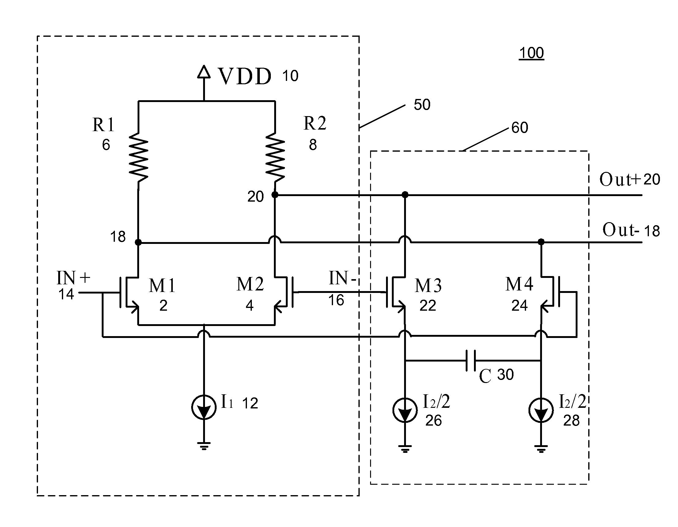
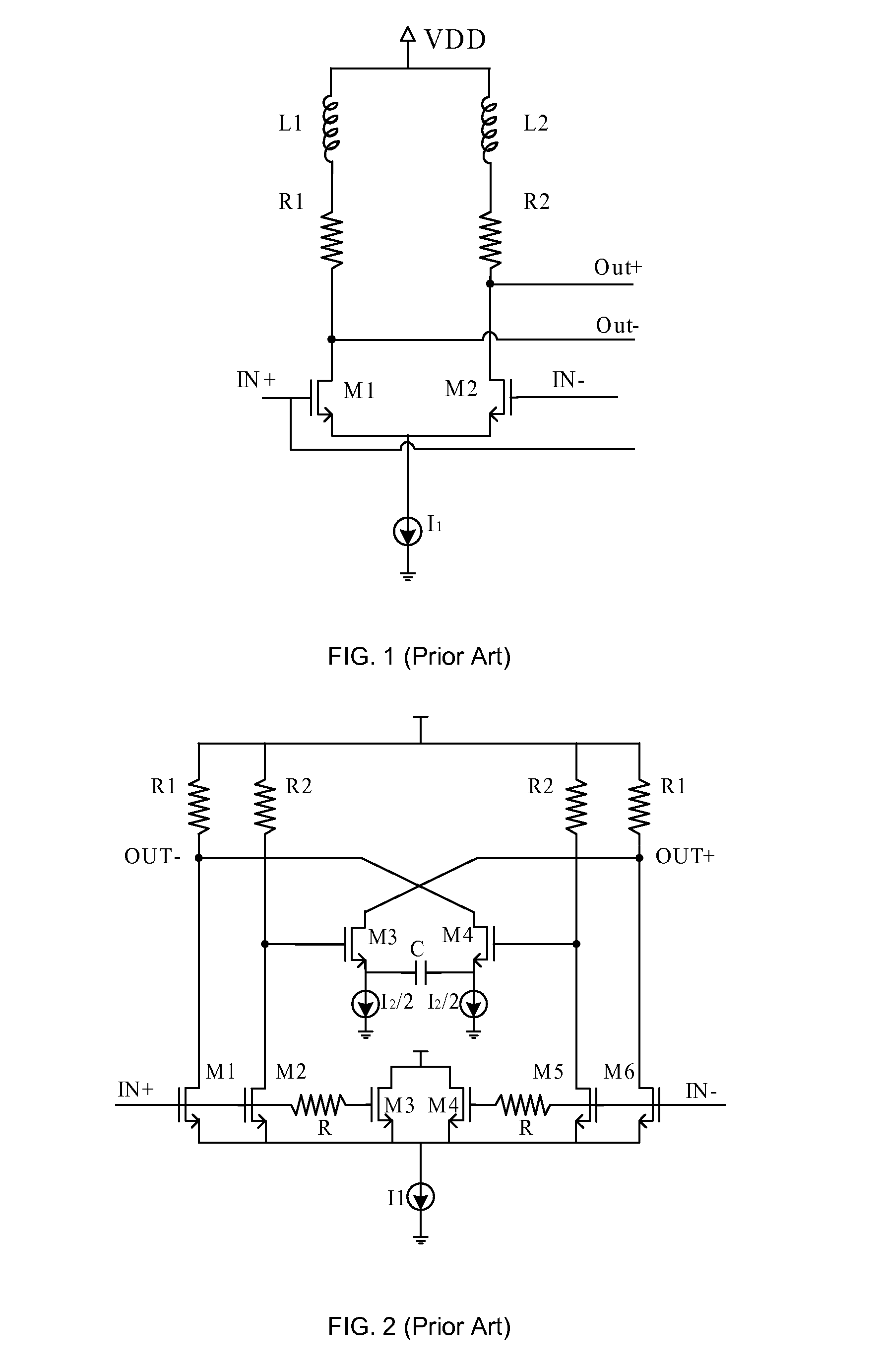
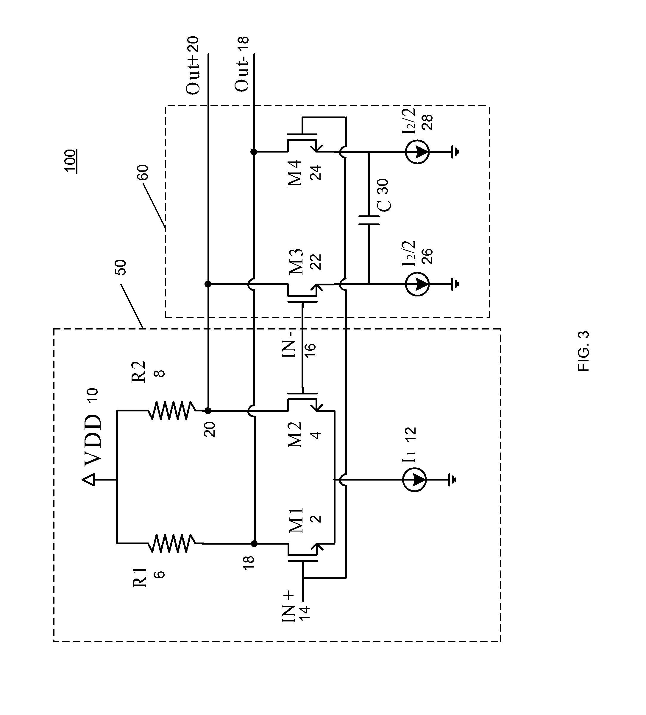
[0010]Systems and methods for actively compensated buffering for high speed current mode logic data paths are disclosed. The following description is presented to enable any person skilled in the art to make and use the invention. Descriptions of specific embodiments and applications are provided only as examples and various modifications will be readily apparent to those skilled in the art. The general principles defined herein may be applied to other embodiments and applications without departing from the spirit and scope of the invention. Thus, the present invention is to be accorded the widest scope encompassing numerous alternatives, modifications and equivalents consistent with the principles and features disclosed herein. For purpose of clarity, details relating to technical material that is known in the technical fields related to the invention have not been described in detail so as not to unnecessarily obscure the present invention.

[0011]Particular circuit layouts and circ...


PUM


Abstract

An actively compensated CML circuit includes a CML buffer circuit and a bandwidth expansion circuit. The CML buffer circuit includes a first MOS transistor and a second MOS transistor in a differential pair configuration. A first load resistor is coupled to a first MOS transistor drain at a first output terminal and a second load resistor is coupled to a second MOS transistor drain at a second output terminal. The bandwidth expansion circuit is coupled to the CML buffer circuit in a source follower configuration. The bandwidth expansion circuit includes a third MOS transistor and a fourth MOS transistor. A capacitor is coupled across a third MOS transistor source and a fourth MOS transistor source. The fourth MOS transistor and the third MOS transistor generate a high pass function at the first output terminal and the second output terminal.

Description

BACKGROUND OF THE INVENTION[0001]As data transfer requirements increase for both on-chip and inter-chip applications, transfer speed remains one of the most critical issues in modern integrated circuit design. Users desire high data transfer speed, but also simultaneously want reduced costs. This speed-cost requirement pushes high speed integrated circuit design to the limits of semiconductor processing. Current mode logic (CML) is widely used in modern high speed data path designs for its superior speed performance. However, CML still encounters speed limitations in multi-giga-bits per second applications.[0002]In the prior art, there have been several techniques used to expand circuit bandwidth. One technique utilizes inductor shunt-peaking. A typical circuit using this technique is illustrated in FIG. 1 and discussed in “The Design of CMOS Radio-Frequency Integrated Circuits”, T. H. Lee, Cambridge University Press, 1998, pp. 146. Referring to FIG. 1, the circuit enhances the CML ...

Claims


Application Information

Patent Timeline
IPC IPC(8): H03K19/094
CPCH03F1/483H03F3/45183H03F2200/36H03F2203/45248H03F2203/45318H03K19/018514H03F2203/45374H03F2203/45638H03F2203/45702H03K19/01707H03F2203/45352
Inventor YU, QUANQU, MING
Owner PARADE TECH
Why Eureka
Try Eureka