Power and Ground Ring Layout

Inactive Publication Date: 2008-02-07
AVAGO TECH WIRELESS IP SINGAPORE PTE
View PDF2 Cites 0 Cited by
  • Summary
  • Abstract
  • Description
  • Claims
  • Application Information

AI Technical Summary

Benefits of technology

[0015]Another aspect of the inventions relates to the shape of the conductive grid patterns. The first and second conductive grid patterns of the IC layout may be square-shaped, rectangular, Manhattan structured, or have some other suitable shape. As the “art” of integrated circuit fabrication advances, it could become possible to efficiently extend conductive grid patterns to have non-right angle turns in the conductive grids.

Problems solved by technology

Generally, the top-down design approach to IC design is the preferred method because the bottom-up design approach is harder to have the chip / system level specification met as lower functional blocks are put together.
This creates complication for power planning engineers to optimally plan the layout of the power grid such that, for example, a minimum IR (voltage) drop is harder to achieve across the IC chip or die, due to package and die size or high level factors that were not considered earlier as in a top-down approach.
IR drop in an IC die can cause signal propagation delays, high average power with the same circuit running speed, and noise created by voltage drops or ground rises in the power and / or ground grids.
However, increasing the density of power grid is not without drawbacks.
The power grid may take up a lot of space in the IC die, thus increasing the size of the die.

Method used


Image

  • Power and Ground Ring Layout
  • Power and Ground Ring Layout
  • Power and Ground Ring Layout

Examples


Embodiment Construction

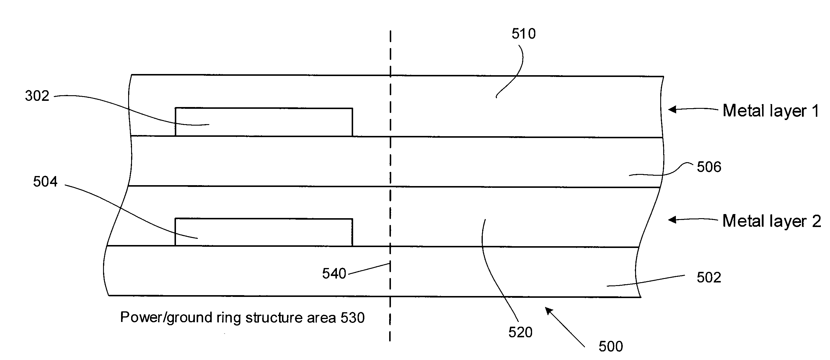
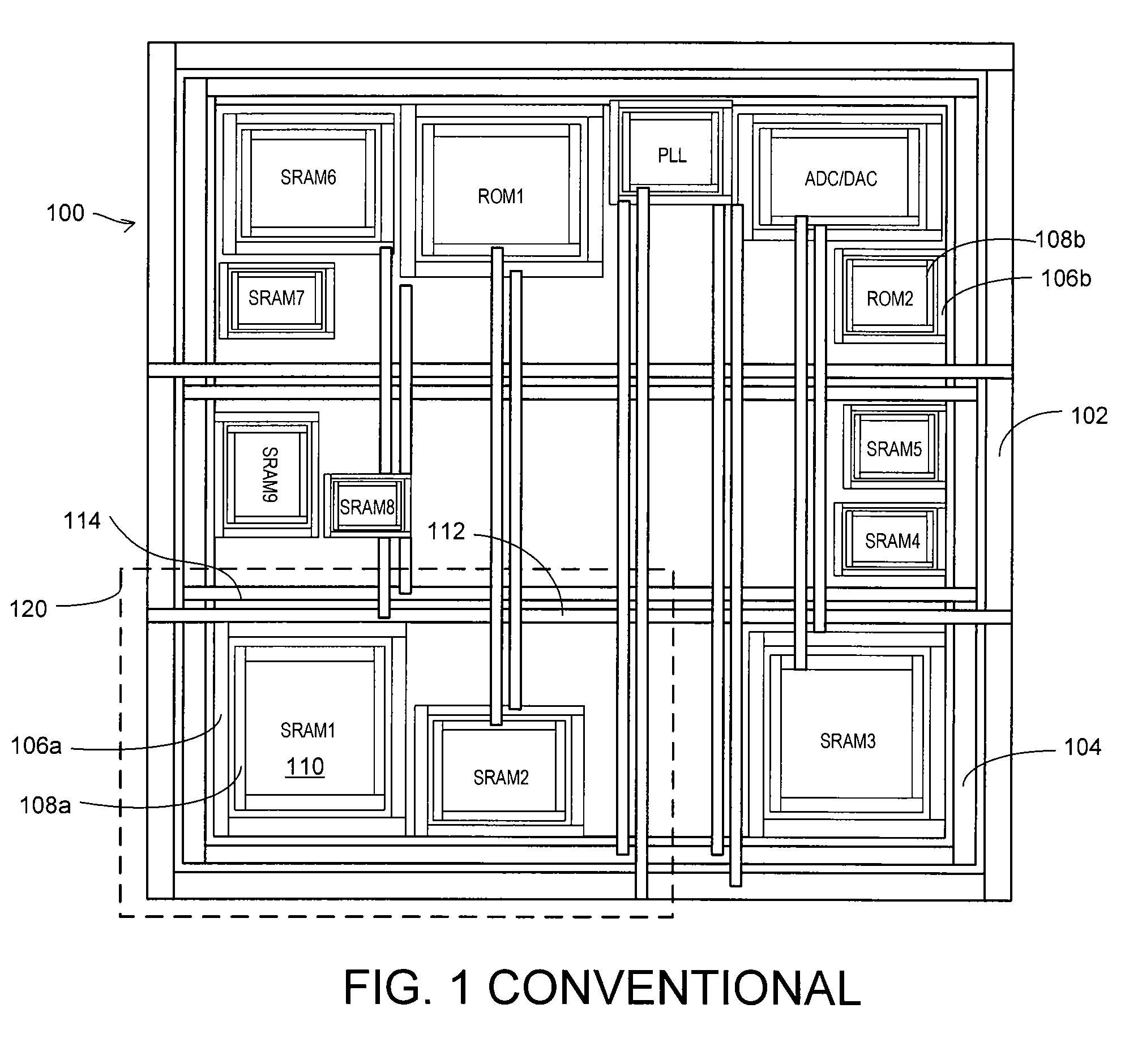
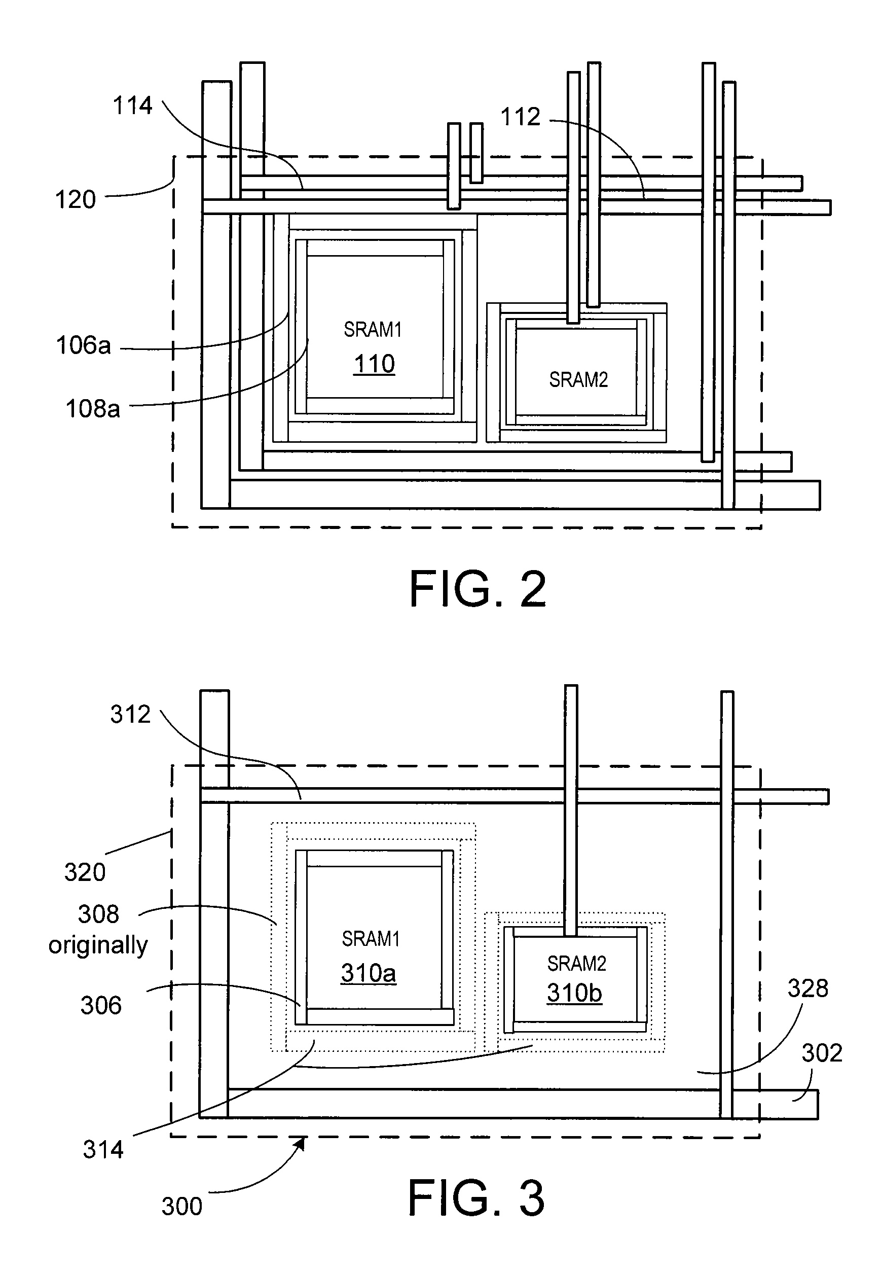
[0028]This specification describes one or more embodiments that incorporate various features of the inventions. The embodiment(s) described, and references in the specification to “one embodiment”, “an embodiment”, “an example embodiment”, etc., indicate that the embodiment(s) described may include a particular feature, structure, or characteristic, but every embodiment may not necessarily include the particular feature, structure, or characteristic. Moreover, such phrases are not necessarily referring to the same embodiment. Further, when a particular feature, structure, or characteristic is described in connection with an embodiment, it is understood that it is within the knowledge of one skilled in the art to effect such feature, structure, or characteristic in connection with other embodiments whether or not explicitly described.

[0029]An embodiment of the inventions is now described. While specific methods and configurations are discussed, it should be understood that this is do...


PUM


Abstract

An integrated circuit layout on a semiconductor substrate includes a plurality of circuit modules and power rails. One of the power rails is a positive voltage supply rail, and another one is a negative voltage supply rail or a ground rail. The positive voltage supply rail is located on a first layer of the semiconductor substrate. The negative voltage supply rail is located on a second layer of the semiconductor substrate. The second layer is located below the first layer. In this way, the integrated circuit layout area is reduced as negative voltage supply rail is moved to another layer.

Description

CROSS-REFERENCE TO RELATED APPLICATION[0001]This application is a Non-Provisional of co-pending U.S. Provisional Application No. 60 / 835,882 filed on Aug. 7, 2006 by Chia-Lang Chang, entitled “POWER AND GROUND RING LAYOUT,” the entire contents of which is hereby incorporated by reference and for which priority is claimed under Title 35, United States Code § 119(e).BACKGROUND OF THE INVENTION[0002]1. Field of the Invention[0003]The inventions relate in general to integrated circuit design. More specifically, the inventions relate to power and ground routing in integrated circuit layout arrangements.[0004]2. Background Art[0005]There are two general methodologies used to determine the arrangements of structures in integrated circuit (IC) chips: top-down and bottom-up methodologies.[0006]In the bottom-up methodology, the layout process is typically as follows. First, circuit gates are designed and arranged. Basic circuit components are then laid out around the gates. Circuit modules are...

Claims


Application Information

Patent Timeline
IPC IPC(8): H01L23/528
CPCH01L23/5286H01L27/0207H01L2924/0002H01L2924/00
Inventor CHANG, CHIA-LANG
Owner AVAGO TECH WIRELESS IP SINGAPORE PTE
Why Eureka
Try Eureka