Liquid crystal display device
a liquid crystal display and display device technology, applied in non-linear optics, instruments, optics, etc., can solve the problem of light leakage at the stepped portion, and achieve the effect of preventing the lowering of a numerical aperture and increasing the transmissivity of the transmissive display region
- Summary
- Abstract
- Description
- Claims
- Application Information
AI Technical Summary
Benefits of technology
Problems solved by technology
Method used
Image

Examples
embodiment 1
[0075]FIG. 1 to FIG. 5 are schematic views showing the schematic constitution of a liquid crystal display panel of an embodiment 1 according to the present invention.
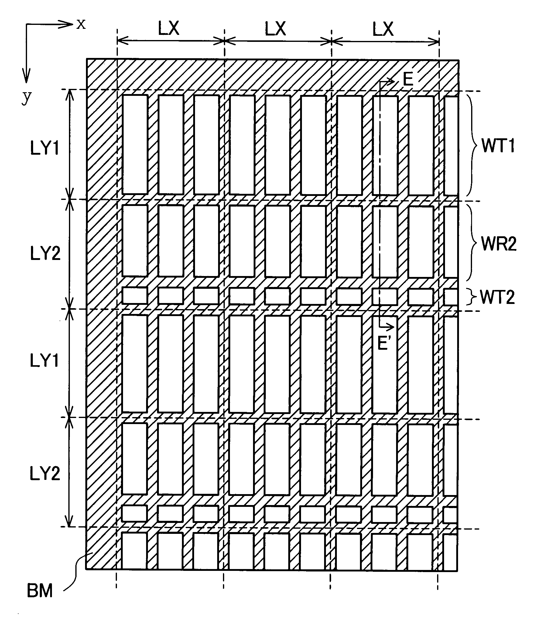
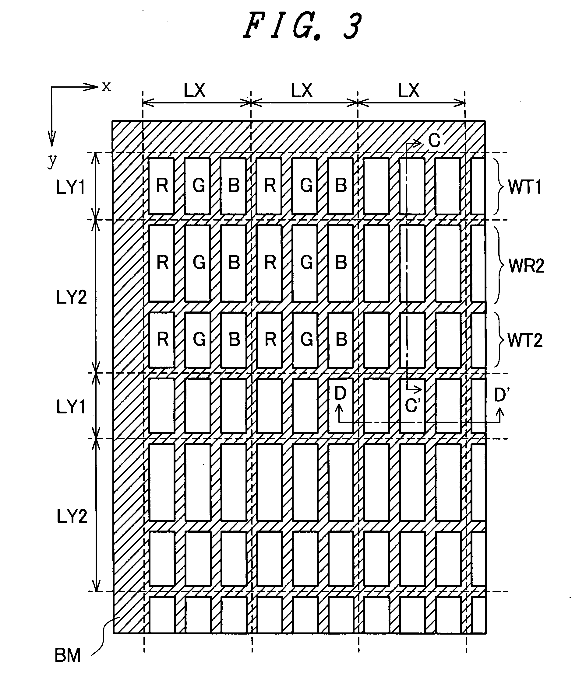
[0076]FIG. 1 is a schematic plan view of the liquid crystal display panel as viewed from a viewer's side. FIG. 2 is a schematic cross-sectional view taken along a line A-A′ in FIG. 1. FIG. 3 is an enlarged schematic plan view of a region AR1 shown in FIG. 1. FIG. 4 is a schematic cross-sectional view taken along a line C-C′ in FIG. 3. FIG. 5 is a schematic cross-sectional view taken along a line D-D′ in FIG. 3.
[0077]In a liquid crystal display panel of this embodiment 1 is, as shown in FIG. 1 and FIG. 2, a liquid crystal material 3 is sealed between a pair of a TFT substrate 1 and a counter substrate 2. Here, the TFT substrate land the counter substrate 2 are, for example, adhered to each other by a sealing material 4 which is annularly provided outside a display region DA, and the liquid crystal material 3 is sealed in...
embodiment 4
[0147]FIG. 15 is a schematic view showing the circuit constitution of one pixel of the liquid crystal display panel of the present invention.
[0148]Although the liquid crystal display panel described in the embodiment 1 or the embodiment 2 includes two kinds of pixels having constitutions different from each other, that is, the first pixels each of which includes only the transmissive display region WT1 and the second pixels each of which includes the reflective display region WR2 and the transmissive display region WT2, both pixels have the circuit constitution shown in FIG. 15. That is, a gate of a TFT element which is arranged with respect to each pixel is connected to one of a plurality of scanning signal lines GL, and a drain of the TFT element is connected to one of a plurality of video signal lines DL. Further, a source of the TFT element is connected to a pixel electrode PX arranged with respect to each pixel. Here, a liquid crystal capacitance Clc is formed between a pixel e...
PUM
 Abstract
Description
Claims
Application Information
 - Generate Ideas
- Intellectual Property
- Life Sciences
- Materials
- Tech Scout
- Unparalleled Data Quality
- Higher Quality Content
- 60% Fewer Hallucinations
Browse by: Latest US Patents, China's latest patents, Technical Efficacy Thesaurus, Application Domain, Technology Topic, Popular Technical Reports.
© 2025 PatSnap. All rights reserved.Legal|Privacy policy|Modern Slavery Act Transparency Statement|Sitemap|About US| Contact US: help@patsnap.com