Package substrate

Active Publication Date: 2008-02-14
UNIMICRON TECH CORP
View PDF6 Cites 6 Cited by
  • Summary
  • Abstract
  • Description
  • Claims
  • Application Information

AI Technical Summary

Benefits of technology

[0008]An objective of the present invention is to provide a package substrate, in which the strength of a thin su

Problems solved by technology

However, as the thickness of the thin substrate is reduced, it cannot provide adequate supportability to meet the flatness requirements.
Particularly, during the bumping process in a

Method used


Image

  • Package substrate
  • Package substrate
  • Package substrate

Examples


Example

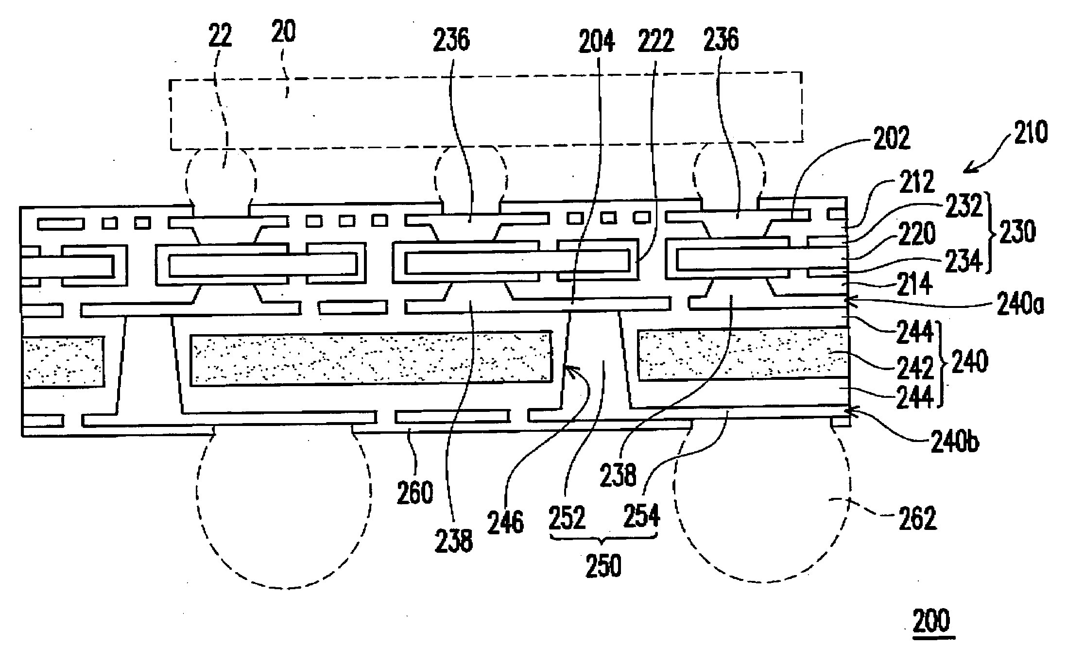
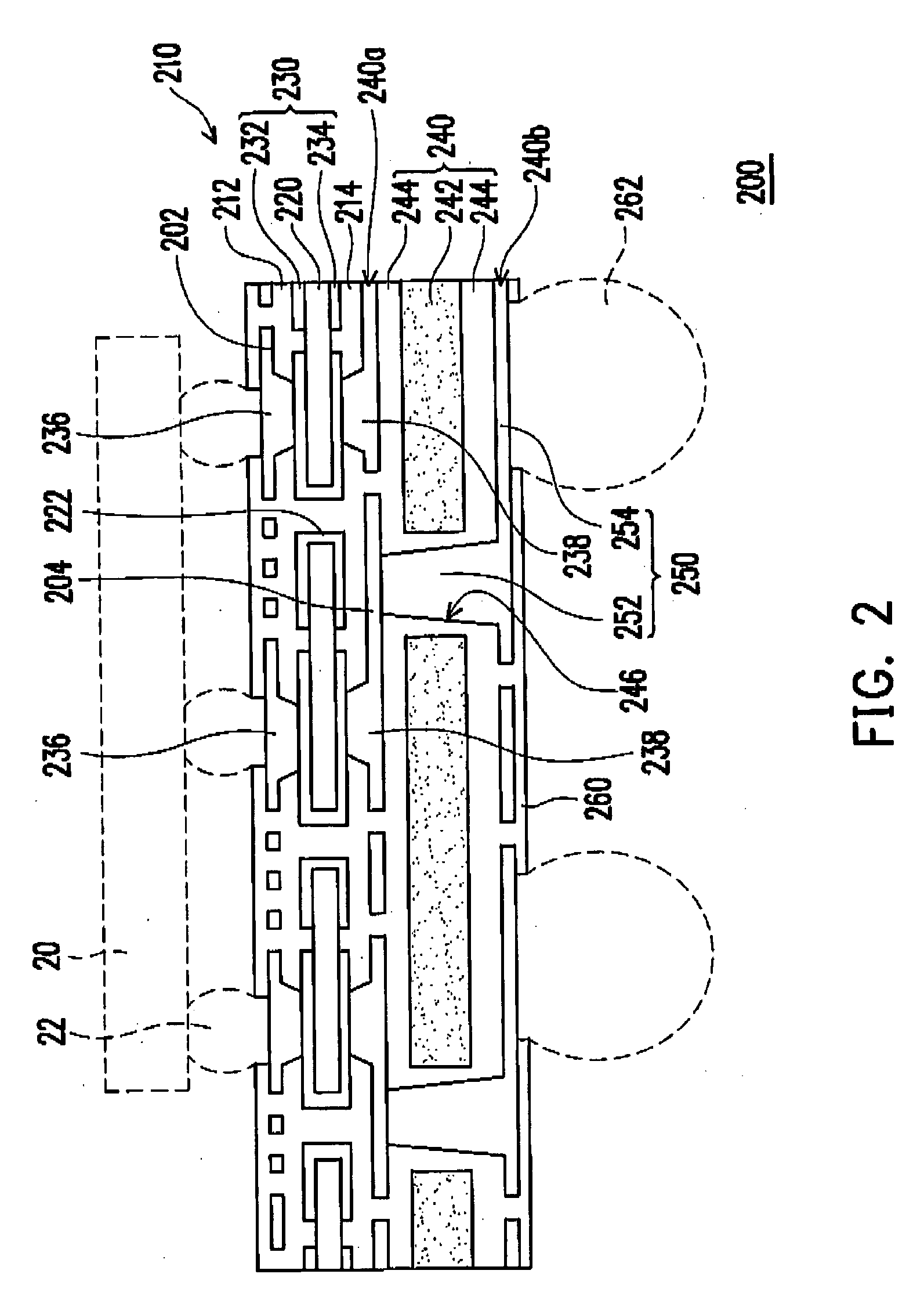
[0017]Referring to FIG. 2, FIG. 2 is a schematic view of a package substrate according to an embodiment of the present invention. The package substrate 200 includes a circuit board 210, which meets the circuit density and thickness limit requirements of a thin substrate, so as to accelerate the transmission of electronic signals. The circuit board 210 has a plurality of upper contacts 202 (i.e., the second contacts), which are correspondingly connected to bumps 22 on a chip 20 (indicated by dashed lines) to transmit the electronic signals. In particular, an inner circuit 230 of the present invention is fabricated by an insulating layer 220 of no glass fiber and by two metal layers formed on two surfaces of the insulating layer 220. The inner circuit 230 includes an upper circuit 232 and a lower circuit 234, which are electrically connected via plated through holes 222 penetrating through the insulating layer 220. The thickness of the insulating layer 220 is less than 100 μm, and is ...


PUM


Abstract

A package substrate including a circuit board, a reinforcing plate and at least one conductive channel is provided. A first surface of the reinforcing plate is disposed on the circuit board for resisting the warpage of the circuit board. The reinforcing plate has an opening corresponding to a first contact of the circuit board exposed thereon. In addition, one end of the conductive channel is located in the opening and electrically connected to the first contact, and the other end of the conductive channel is located on a second surface of the reinforcing plate to form a bonding pad.

Description

CROSS-REFERENCE TO RELATED APPLICATION[0001]This application claims the priority benefit of Taiwan application serial no. 95129187, filed Aug. 9, 2006. All disclosure of the Taiwan application is incorporated herein by reference.BACKGROUND OF THE INVENTION[0002]1. Field of Invention[0003]The present invention relates to a package substrate, and more particularly, to a package substrate in which the structural strength of a thin circuit board is reinforced.[0004]2. Description of Related Art[0005]In recent years, as the rapid progress of the electronic technology, high-tech electronic products have been developed, thus human-oriented electronic products with preferred performance have brought forth a new era, and have been designed to cater to the trend of being light, thin, short, and small.[0006]Referring to FIG. 1, FIG. 1 is a schematic view of a conventional package substrate. To enhance the strength of a package substrate 100, a copper foil substrate 120 with a core layer 110 co...

Claims


Application Information

Patent Timeline
IPC IPC(8): H01L23/02
CPCH01L23/49816H01L23/49833H05K1/056H05K3/4608H05K3/4641H01L2924/15311H05K2201/0949H05K2201/09536H05K2201/10674H01L2224/16225H05K2201/09481H01L2924/00014H01L2924/00011H01L2224/0401
Inventor CHENG, DAVID C. H.
Owner UNIMICRON TECH CORP
Why Eureka
Try Eureka