Method and system for minimizing number of programming pulses used to program rows of non-volatile memory cells

a non-volatile memory cell and programming pulse technology, applied in the field of non-volatile memory devices, can solve the problems of limiting the precision with which circuitry can store analog values on the floating gate of flash cells, flash cells across an array and even across a single row may not all behave the same, and it is not economically feasible to manufacture memory devices without any defects

Active Publication Date: 2008-02-21
MICRON TECH INC
View PDF68 Cites 103 Cited by
  • Summary
  • Abstract
  • Description
  • Claims
  • Application Information

AI Technical Summary

Problems solved by technology

As a result of the very large number of components in high capacity memory devices, including flash memory devices, it is not economically feasible to manufacture memory devices without any defects.
There is also a limit to the precision with which circuitry can store an analog value on the floating gate of a flash cell, particularly where multiple levels of charge must be stored.
In particular, because of process variations, the flash cells across an entire array and even across a single row may not all behave identically.
As can be appreciated, it can require a considerable period of time to program flash memory cells in this iterative manner.
This problem is particularly acute for multi-level flash memory cells.
However, these conventional ECC techniques are usually limited to repairing a relatively small number of data bit errors in each row.
As explained above, this can adversely affect the programmed state of previously programmed cells.
Although this problem is described in the context of flash memory devices, it also exists in other types of non-volatile memory devices.

Method used


Image

  • Method and system for minimizing number of programming pulses used to program rows of non-volatile memory cells
  • Method and system for minimizing number of programming pulses used to program rows of non-volatile memory cells
  • Method and system for minimizing number of programming pulses used to program rows of non-volatile memory cells

Examples


Embodiment Construction

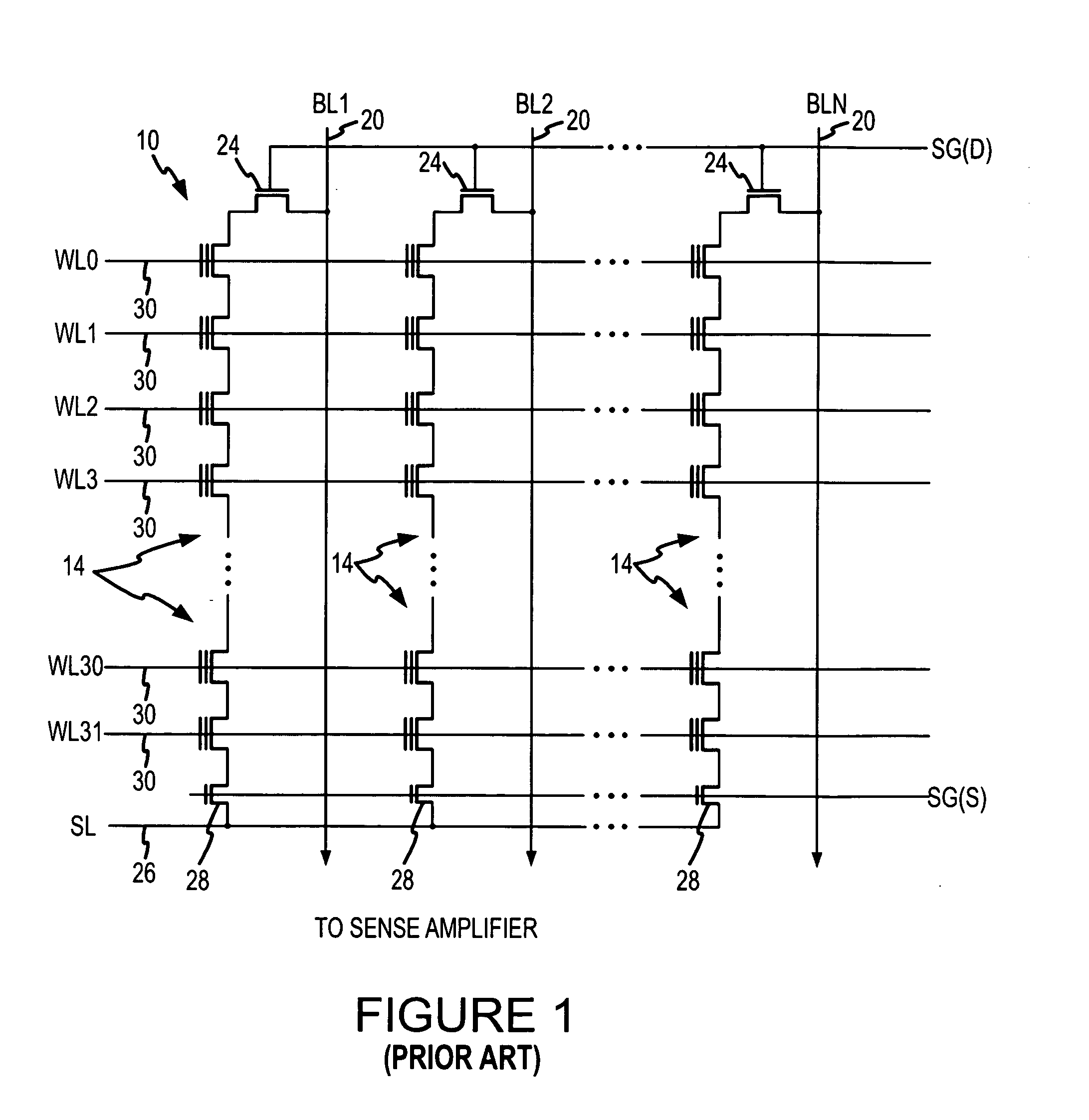
[0025]A flash memory device 100 of conventional design that can be used according to one example of the invention is shown in FIG. 3. The flash memory device 100 includes an array 130 of flash memory cells arranged in banks of rows and columns. The flash memory cells in the array 130 have their control gates coupled to word select lines, drain regions coupled to local bit lines, and source regions selectively coupled to a ground potential as shown in FIG. 1.

[0026]Unlike conventional dynamic random access memory (“DRAM”) devices and static random access memory (“SRAM”) devices, command, address and write data signals are not applied to the flash memory device 100 through respective command, address and data buses. Instead, most command signals, the address signals and the write data signals are applied to the memory device 100 as sets of sequential input / output (“I / O”) signals transmitted through an I / O bus 134. Similarly, read data signals are output from the flash memory device 100...


PUM


Abstract

A flash memory device programs cells in each row in a manner that minimizes the number of programming pulses that must be applied to the cells during programming. The flash memory device includes a pseudo pass circuit that determines the number of data errors in each of a plurality of subsets of data that has been programmed in the row. The size of each subset corresponds to the number of read data bits coupled from the memory device, which are simultaneously applied to error checking and correcting circuitry. During iterative programming of a row of cells, the pseudo pass circuit indicates a pseudo pass condition to terminate further programming of the row if none of the subsets of data have a number of data errors that exceeds the number of data errors that can be corrected by the error checking and correcting circuitry.

Description

TECHNICAL FIELD[0001]This invention relates to non-volatile memory devices, and, more particularly, to a non-volatile memory device in which the number of programming pulses used to program a row of non-volatile memory cells is limited to the number required to program a sufficient number of cells that any data errors can be corrected by error checking and correcting means.BACKGROUND OF THE INVENTION[0002]Electrically erasable and programmable memory devices having arrays of flash memory cells are found in a wide variety of electrical devices. A flash memory cell, also known as a floating gate transistor memory cell, is similar to a field effect transistor, having a source region and a drain region that is spaced apart from the source region to form an intermediate channel region. A floating gate, typically made of doped polysilicon, is disposed over the channel region and is electrically isolated from the channel region by a layer of gate oxide. A control gate is fabricated over th...

Claims


Application Information

Patent Timeline
Patent Type & Authority Applications(United States)
IPC IPC(8): G11C11/34
CPCG11C8/10G11C16/10G11C16/3436G11C7/16
Inventor ROOHPARVAR, FRANKIE
Owner MICRON TECH INC
Why Eureka
Try Eureka