MEMS optical switch device

a technology of optical switch and optical switch device, which is applied in the field can solve the problems of increasing device size, detecting abnormalities, and increasing cost, so as to reduce the number of light sources and reduce the cost and size of mems optical switch devi

Inactive Publication Date: 2008-02-28
FUJITSU LTD
View PDF15 Cites 24 Cited by
  • Summary
  • Abstract
  • Description
  • Claims
  • Application Information

AI Technical Summary

Benefits of technology

[0017]According to one aspect of the present invention, it is possible to significantly reduce the number of light sources

Problems solved by technology

However, according to the conventional MEMS optical switch of Patent Document 1, the light sources of test light are connected to all the input ports and the output levels of all th

Method used


Image

  • MEMS optical switch device
  • MEMS optical switch device
  • MEMS optical switch device

Examples


Embodiment Construction

[0025]A description is given below, with reference to the accompanying drawings, of an embodiment of the present invention.

[0026][Configuration of MEMS Optical Switch Device]

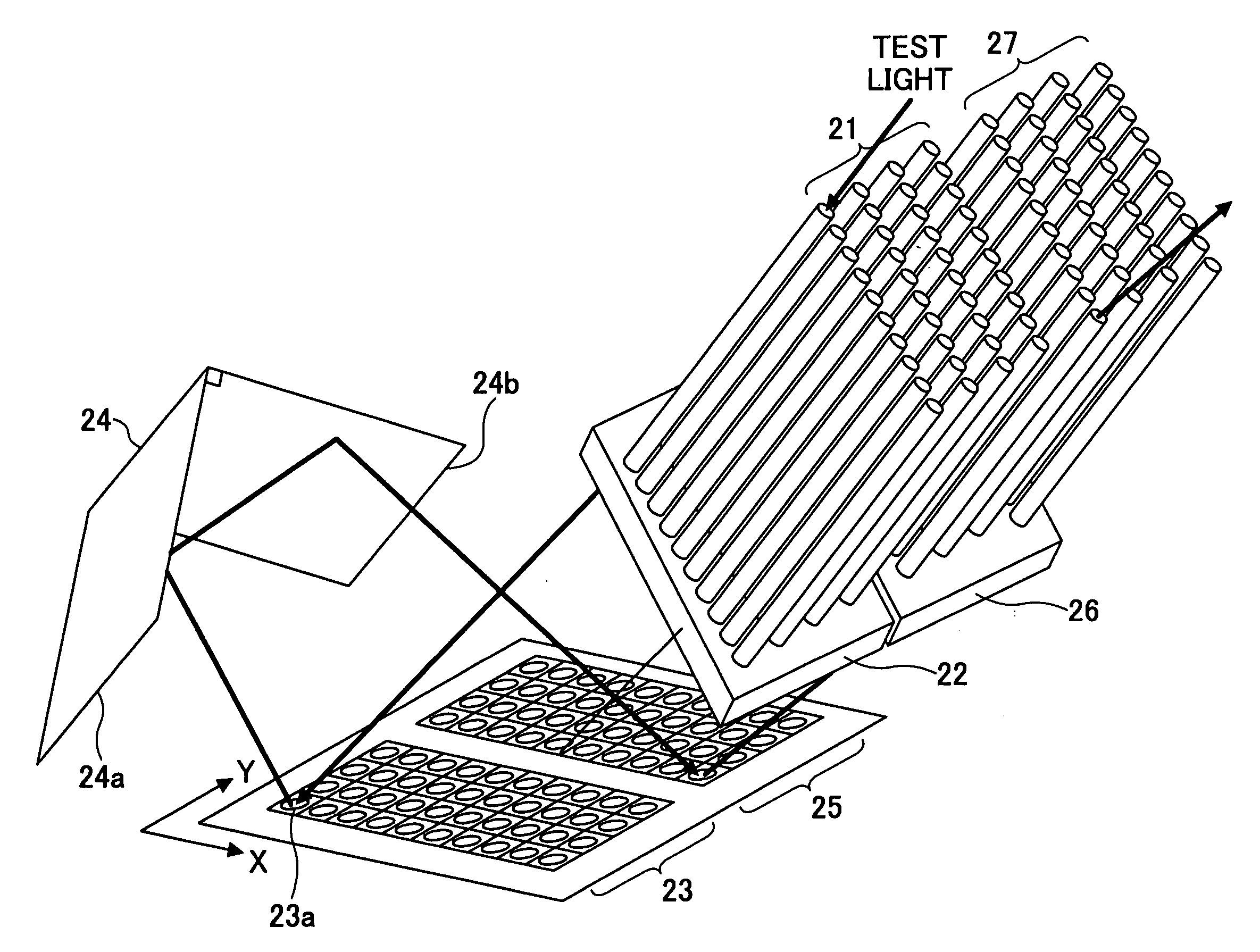
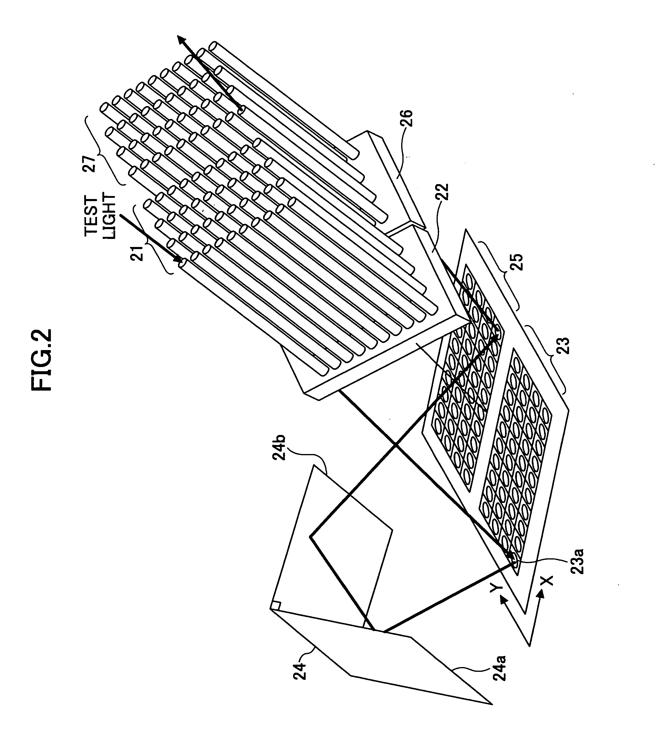
[0027]According to a MEMS optical switch device of this embodiment, a light signal input from one of multiple input ports is subjected to switching on a channel-by-channel basis so as to be output selectively from an output port assigned to the one of the input ports. Here, a light signal input to one input port is referred to as one channel irrespective of whether the input light signal is a single-wavelength or WDM signal.

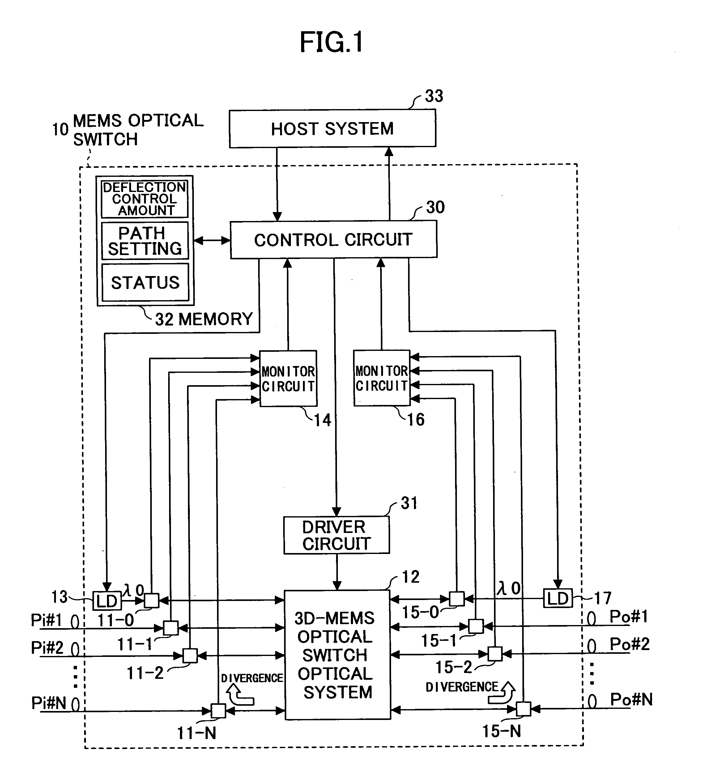
[0028]FIG. 1 is a block diagram showing a MEMS optical switch device 10 according to the embodiment of the present invention. Referring to FIG. 1, the MEMS optical switch device 10 has light signals of N channels input thereto from the optical fibers of corresponding input ports Pi#1 through Pi#N. These light signals are fed to a three-dimensional MEMS optical switch optical system 12 through...


PUM


Abstract

A MEMS optical switch device is disclosed that includes an optical system deflecting and outputting light signals; first and second test light generation parts generating and feeding first and second test lights to specific input and output ports, respectively, of the optical system; first and second divergence parts diverging the first and second test lights, respectively, from the optical system; first and second monitoring parts detecting the diverged first and second test lights, respectively; and an operational check part causing the first and second test lights to be incident on output and input deflection parts of the optical system by driving a specific input deflection part corresponding to the specific input port and a specific output deflection part corresponding to the specific output port, respectively, and performing an operational check on the output and input deflection parts from the light levels of the detected first and second test lights, respectively.

Description

BACKGROUND OF THE INVENTION[0001]1. Field of the Invention[0002]The present invention relates generally to MEMS (Micro Electro Mechanical Systems) optical switch devices, and more particularly to a MEMS optical switch device that is an optical switch using a MEMS mirror.[0003]2. Description of the Related Art[0004]Wavelength division multiplexing (WDM) is an effective technique for constituting a large-capacity optical communications network, and WDM traffic has been exploding these days with the explosive spread of the Internet.[0005]A common optical cross-connect (OXC) system as a backbone optical network according to WDM is formed of multiple optical signal exchangers interconnected by optical fibers. When a WDM light signal is input to the optical signal exchanger through an optical fiber, the optical signal exchanger switches the route of the light signal wavelength by wavelength, and can transmit light signals in the same route in the form of a WDM light signal.[0006]According...

Claims


Application Information

Patent Timeline
IPC IPC(8): G02B6/26
CPCG02B6/3512G02B6/3556G02B6/359H04Q2011/0083H04Q2011/003H04Q2011/0039H04Q2011/0049H04Q11/0005
Inventor SAKAI, YOSHIOMORI, KAZUYUKI
Owner FUJITSU LTD
Why Eureka
Try Eureka