Electrooptical device and electronic apparatus

a technology of electronic equipment and optical components, applied in the field of optical components, to achieve the effect of reducing or eliminating the size of the front region with a mixed display

Inactive Publication Date: 2008-03-06
JAPAN DISPLAY WEST
View PDF5 Cites 24 Cited by
  • Summary
  • Abstract
  • Description
  • Claims
  • Application Information

AI Technical Summary

Benefits of technology

[0010]An advantage of some aspects of the invention is that the size front region with a mixed display is reduced or eliminated while maintaining the brightness of the first and second image.

Problems solved by technology

One disadvantage of the current configuration, however, is that in the angle range VC, a mixture of the first image and the second image is displayed, rather than one complete image.

Method used


Image

  • Electrooptical device and electronic apparatus
  • Electrooptical device and electronic apparatus
  • Electrooptical device and electronic apparatus

Examples


first exemplary embodiment

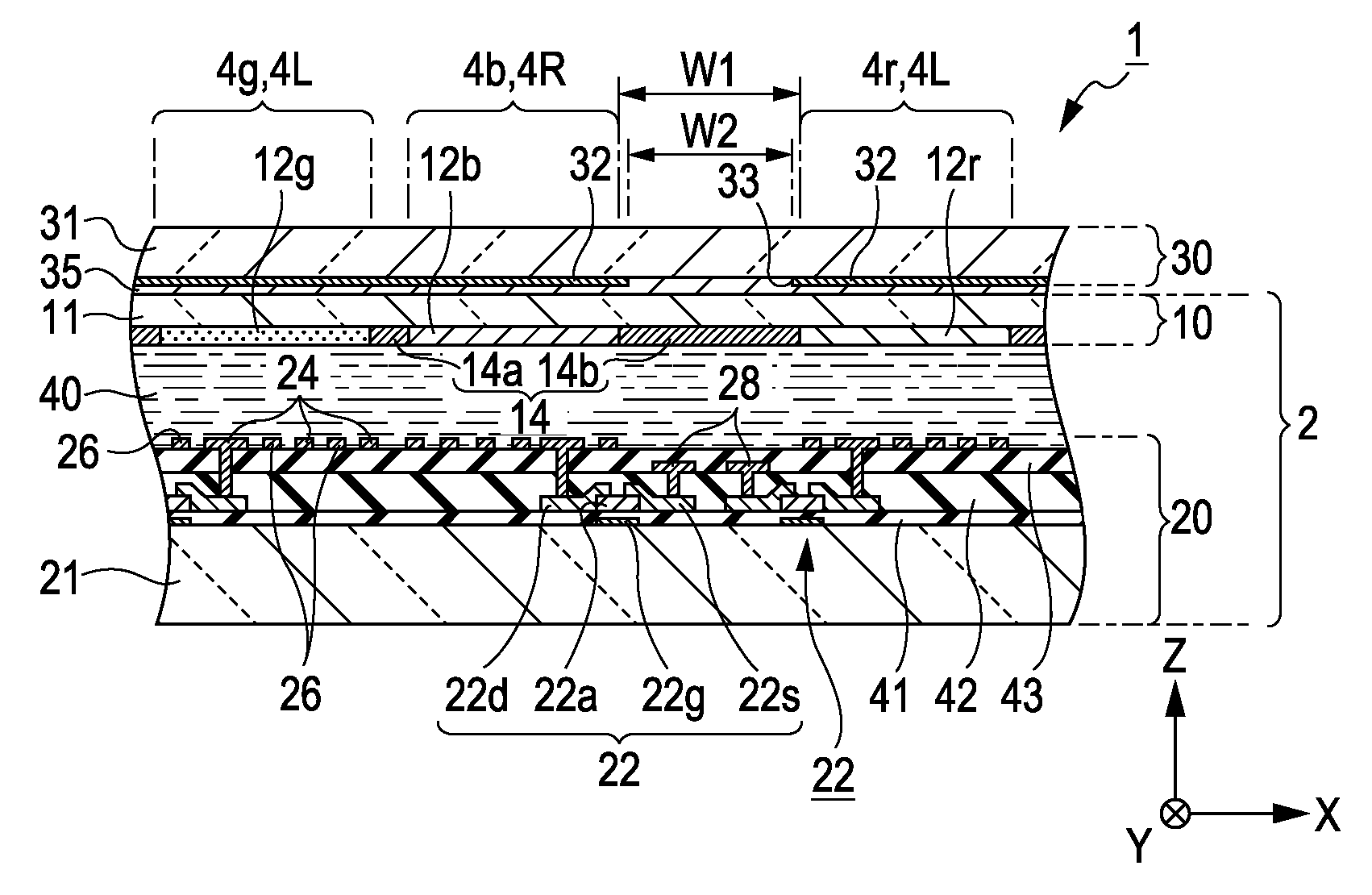
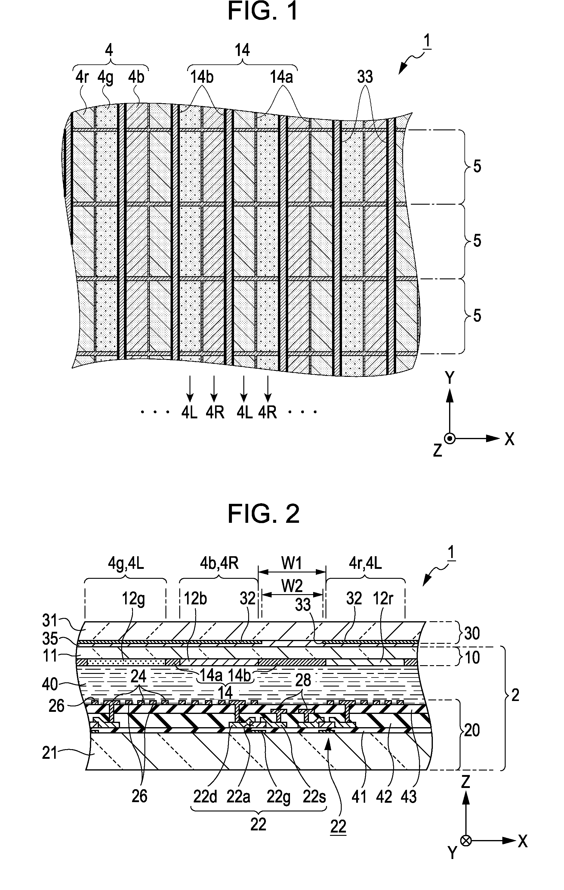
[0030]FIG. 1 is an enlarged plan view of a liquid crystal device 1, which serves as an electrooptical device according to a first exemplary embodiment of the invention. FIG. 2 is a cross-sectional view of the liquid crystal device 1 shown in FIG. 1. As shown in FIG. 2, the liquid crystal device 1 includes a liquid crystal panel 2 which serves as a display panel. A barrier mask substrate 30 is bonded to the liquid crystal panel 2 with an adhesive 35. The barrier mask substrate 30 includes a glass substrate 31, and a light-shielding barrier layer 32 provided on a surface of the glass substrate 31, which faces the liquid crystal panel 2. The glass substrate 31 is disposed parallel to the liquid crystal panel 2. The barrier layer 32 is formed of a black resin layer and has apertures 33.

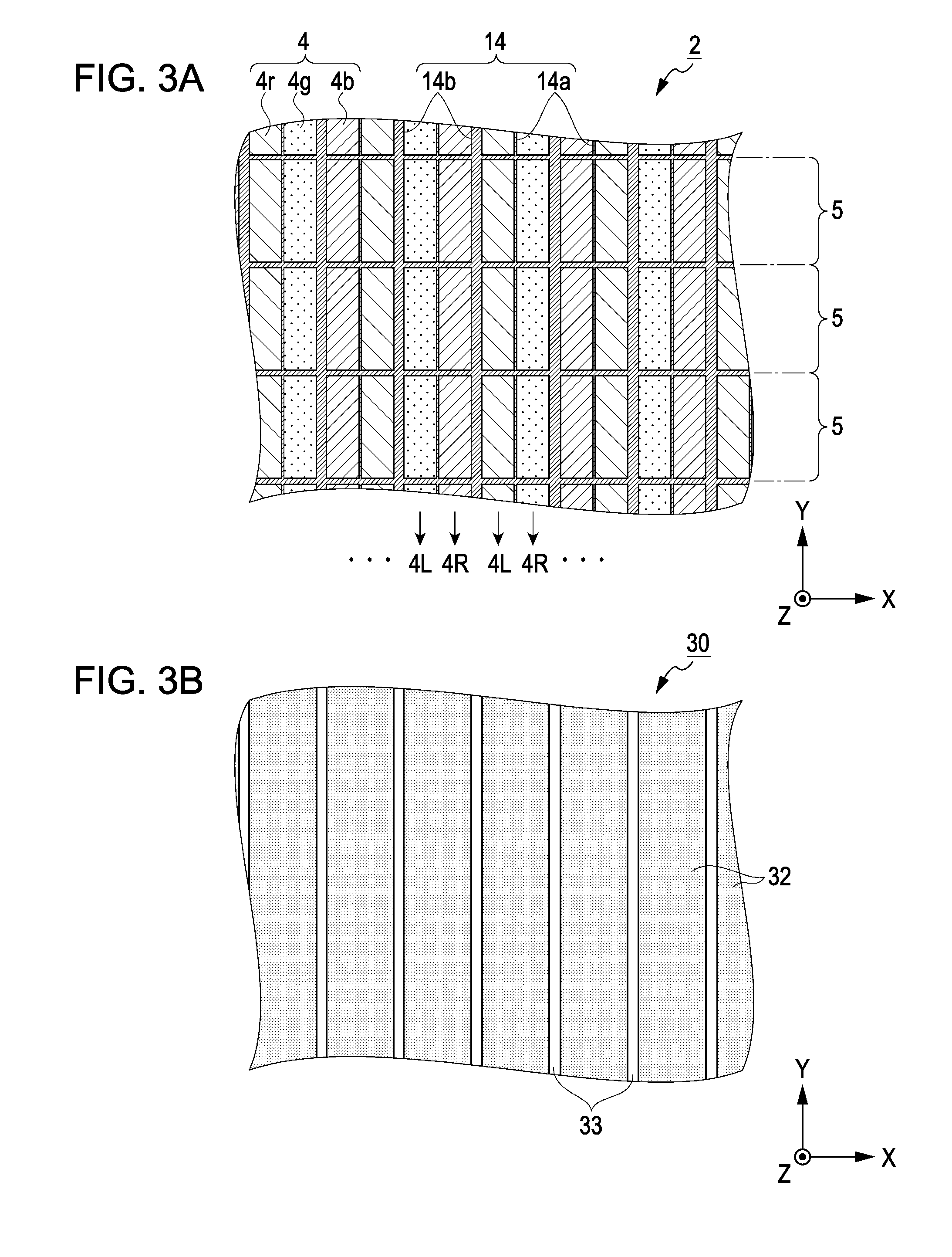
[0031]FIGS. 3A and 3B are enlarged views of the liquid crystal panel 2 and the barrier mask substrate 30 before bonding, respectively. The liquid crystal panel 2 and the barrier mask substrate 30 are bond...

second exemplary embodiment

[0053]A liquid crystal device 1A according to a second exemplary embodiment of the invention will now be described with reference to FIGS. 5 and 6. The liquid crystal device 1A differs from the liquid crystal device 1 of the first exemplary embodiment in the arrangement of pixels 4L, 4R, light-shielding layers 14a and 14b, and apertures 33. Since other structures are similar to those in the liquid crystal device 1, the following description will center on differences. In FIGS. 5 and 6, the same components as those in the first exemplary embodiment shown in FIGS. 1 and 3 are denoted by the same reference numerals, and descriptions thereof are omitted.

[0054]FIG. 5 is an enlarged plan view of the liquid crystal device 1A according to the second exemplary embodiment. Similar to the liquid crystal device 1 of the first exemplary embodiment, the liquid crystal device 1A includes a liquid crystal panel 2A which serves as a display panel and a barrier mask substrate 30A bonded together with...

third exemplary embodiment

[0062]A liquid crystal device 1B according to a third exemplary embodiment of the invention will now be described with reference to FIGS. 7 and 8. The liquid crystal device 1B differs from the liquid crystal device 1 of the first exemplary embodiment in the width of apertures 33 provided in the barrier layer 32. Since the other structures are similar to those in the liquid crystal device 1, the following description will center on differences. In FIGS. 7 and 8, the same components as those in the first exemplary embodiments shown in FIGS. 1 and 4 are denoted by the same reference numerals, and descriptions thereof are omitted.

[0063]FIG. 7 is an enlarged plan view of the liquid crystal device 1B according to the third exemplary embodiment. Similarly to the liquid crystal device 1, the liquid crystal device 1B includes a liquid crystal panel 2B serving as a display panel and a barrier mask substrate 30B that are bonded together with adhesive 35, as shown in FIG. 8. Hatched portions in...


PUM

PropertyMeasurementUnit
thicknessaaaaaaaaaa
thicknessaaaaaaaaaa
thicknessaaaaaaaaaa

Abstract

An electrooptical device which simultaneously displays a first and second image in different directions. The electrooptical device includes a display panel including a plurality of pixel rows. Each pixel row includes first pixels for displaying the first image, first light-shielding portions, second pixels for displaying the second image, and second light-shielding portions which are wider than the first light-shielding portions. The electrooptical device also includes a light-transmissive substrate provided parallel to the display panel, and a light-shielding barrier layer provided on the substrate which includes apertures that align with the second light-shielding portions when viewed from a direction that is normal to the display panel.

Description

BACKGROUND[0001]The entire disclosure of Japanese Patent Application No. 2006-241119, filed Sep. 9, 2006 is expressly incorporated herein by reference.[0002]1. Technical Field[0003]The present invention relates to electrooptical devices. More specifically, the present invention relates to an electronic apparatus capable of simultaneously displaying two images in different directions.[0004]2. Related Art[0005]Electrooptical devices which are capable of simultaneously displaying two images in different directions are known in the art. Typically, such devices include a display panel, such as a liquid crystal panel, which includes a light-shield barrier layer with a number of light apertures. One example of such a device is found in Japanese Patent No. 2,857,429, which discloses a three-dimensional image display device which is capable of creating a three-dimensional display with two images.[0006]FIG. 10 is an enlarged view of a liquid crystal device 6 which serves an electrooptical dev...

Claims


Application Information

Patent Timeline
Patent Type & Authority Applications(United States)
IPC IPC(8): G02F1/133
CPCG02B27/2214H04N13/0409G02F1/133512H04N13/31G02F1/13471G02B30/27
Inventor MAEDA, TSUYOSHI
Owner JAPAN DISPLAY WEST
Why Eureka
Try Eureka