Packaging board, semiconductor module, and portable apparatus

a technology of semiconductor modules and packaging boards, applied in electrical devices, semiconductor devices, semiconductor/solid-state device details, etc., can solve the problems of affecting the reliability of connection, and b>500/b> lack of handleability in the steps of handling printed circuit boards, etc., to achieve the effect of improving handleability and ensuring connection reliability

Inactive Publication Date: 2008-03-13
SANYO ELECTRIC CO LTD
View PDF7 Cites 21 Cited by
  • Summary
  • Abstract
  • Description
  • Claims
  • Application Information

AI Technical Summary

Benefits of technology

[0013] The present invention has been achieved in view of the foregoing circumstances, and it is thus a general...

Problems solved by technology

Since the solder coating 54 protruding in this way impairs the flatness of the printed circuit board 500 at the surface, there has been the problem that the printed circuit board 500 lacks handleability in the steps of handling the printed circuit board 500 listed below.
This produces a...

Method used


Image

  • Packaging board, semiconductor module, and portable apparatus
  • Packaging board, semiconductor module, and portable apparatus
  • Packaging board, semiconductor module, and portable apparatus

Examples


first embodiment

[0042] Hereinafter, a first embodiment of the packaging board according to the present invention will be described with reference to FIGS. 1 and 2.

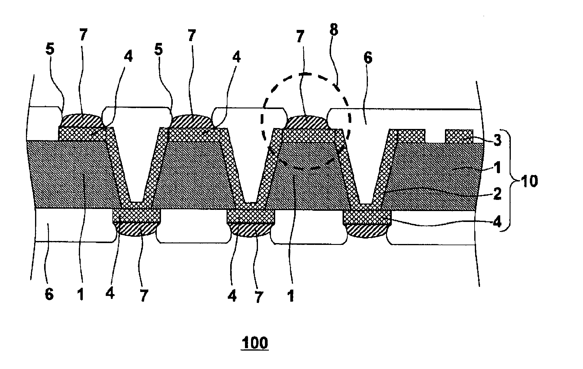
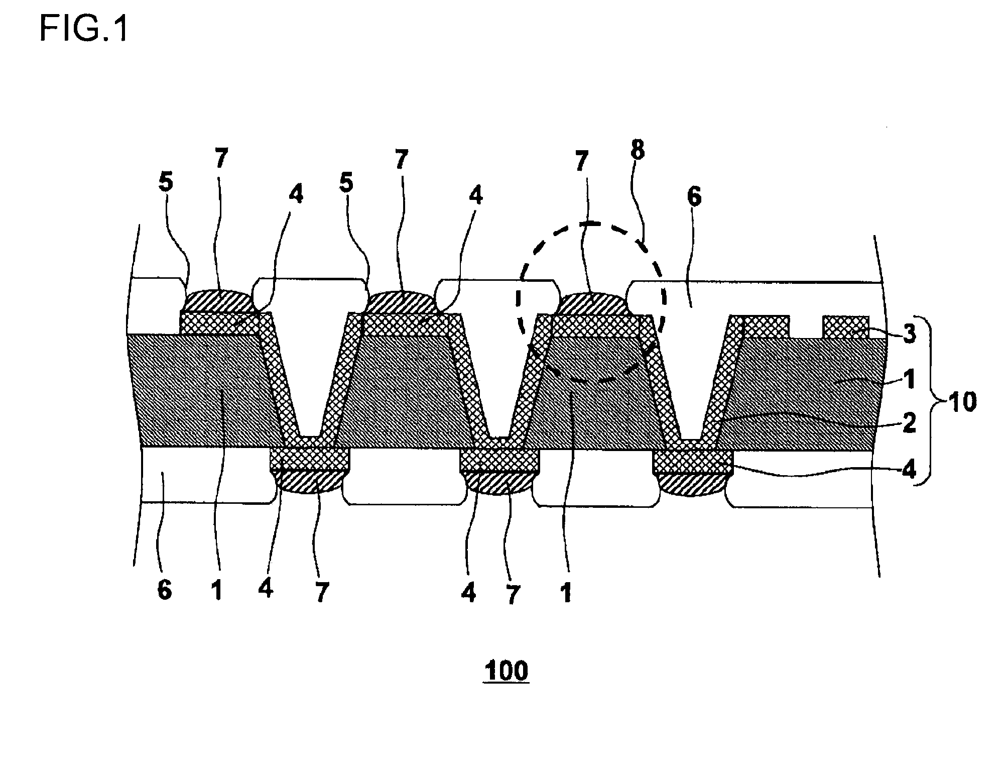
[0043] Initially, referring to FIG. 1, the structure of the packaging board 100 according to the present embodiment will be described in detail. FIG. 1 shows a cross-sectional view of the packaging board 100. A substrate 1 is provided with wiring parts 2. A wiring pattern 3 and pad electrodes 4 made of copper (Cu) are formed on the surface of the substrate 1. The pad electrodes 4 are electrically connected to the wiring parts 2. A wiring board 10 is composed of the substrate 1, the wiring parts 2, the wiring pattern 3, and the pad electrodes 4 mentioned above.

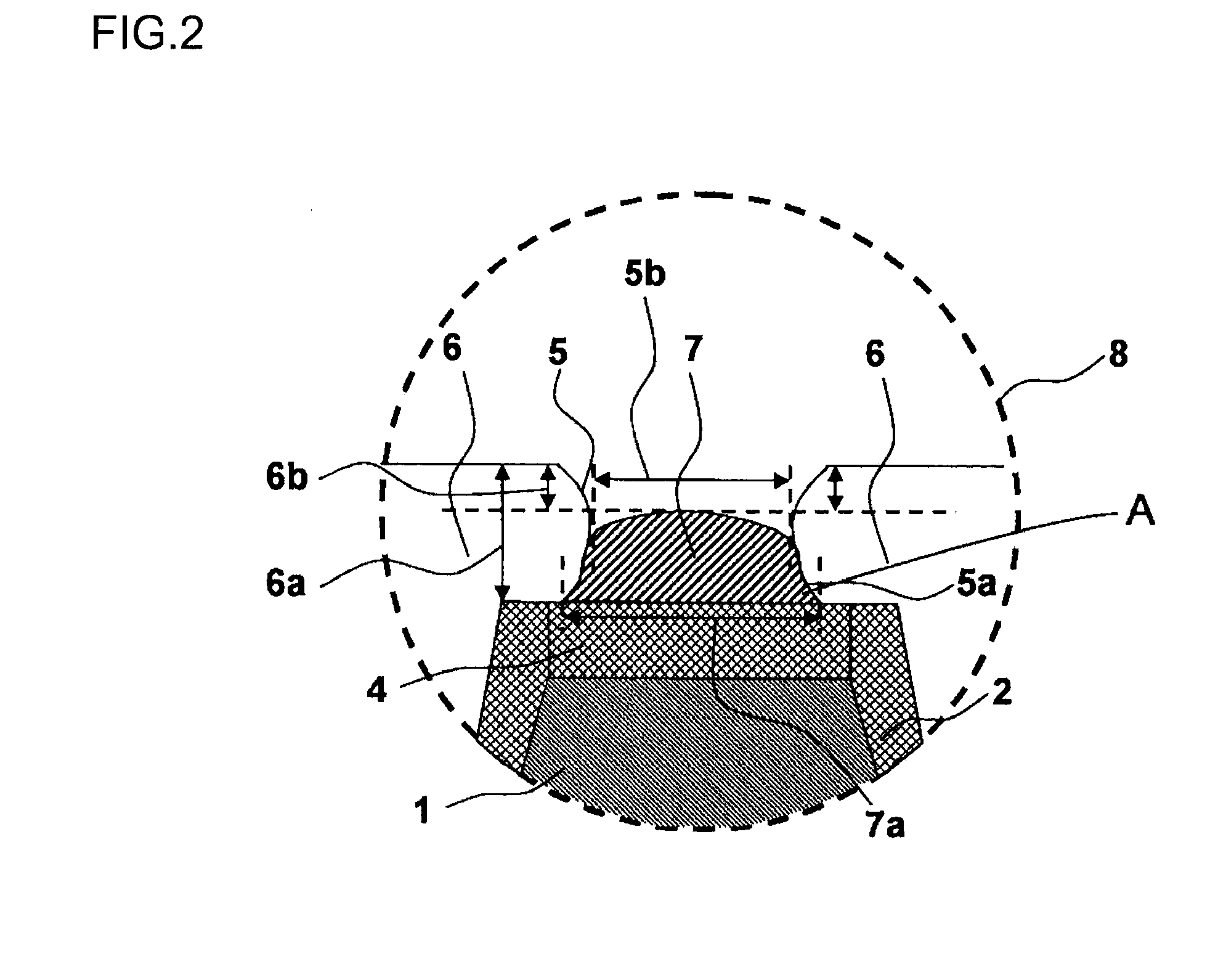
[0044] The surface of the wiring board 10 is coated with a solder resist layer 6. Openings 5 are formed in the solder resist layer 6 at positions corresponding to the top surfaces of the pad electrodes 4. The solder resist layer 6 functions as a protective coating for the wiring pa...

second embodiment

[0069] A description will now be given of a second embodiment of the packaging board according to the present invention. The packaging board of the present embodiment also has a basic structure conforming to the packaging board of the foregoing first embodiment. A difference, however, consists in that the packaging board according to the present embodiment has a plurality of wiring boards. This packaging board will be described with reference to FIG. 8. It should be noted that the same or similar structures as in the foregoing first embodiment will be designated by like reference numerals, and detailed description thereof will be omitted.

[0070]FIG. 8 shows a cross-sectional view of the packaging board 200. A multilayered wiring board 20 is composed of a substrate 11, insulating layers 13 and 15, and conductive layers 12, 14, and 16. The conductive layer 12 made of copper (Cu) is formed on the substrate 11. A first insulating layer 13 consisting mainly of epoxy resin, having a thick...

third embodiment

[0103]FIG. 14 is a sectional view showing the structure of a semiconductor module 310 which has LSI chips mounted on a packaging board 300 according to a third embodiment. The semiconductor module 310 of the present embodiment includes circuit devices 18c and 18d such as an LSI, and passive elements 319 such as a resistor and a capacitor. Initially, a description will be given of the structure of the packaging board 300. A wiring layer 303 is patterned on an insulating layer 302, a core member. For flip-chip connection, flip-chip pads 305 having a nickel gold plating layer 304 are formed in the center area of the packaging board 300. Solder bumps 312 are formed on the nickel gold plating layer 304.

[0104] For wire bonding connection, wire bonding pads 306 having a nickel metal plating layer 304 are arranged around the flip-chip pads 305. Moreover, for the purpose of mounting the passive elements 319, passive element pads 320 having a nickel metal plating layer 304 are arranged aroun...


PUM


Abstract

A technology is provided for a packaging board adapted to mount a device capable of improving handleability and securing connection reliability. The packaging board includes: a pad electrode formed on a substrate; an insulating layer covering the substrate, having an opening at least in part in an area over the pad electrode; and a joint layer formed on the pad electrode inside the opening. The surface of the joint layer is lower than the top lip of the opening.

Description

CROSS-REFERENCE TO RELATED APPLICATIONS [0001] This application is based upon and claims the benefit of priority from the prior Japanese Patent Application No. 2006-234465, filed Aug. 30, 2006, and Japanese Patent Application No. 2007-211172, filed Aug. 13, 2007, the entire contents of which are incorporated herein by reference. BACKGROUND OF THE INVENTION [0002] 1. Field of the Invention [0003] The present invention relates to a packaging board, a semiconductor module, and a portable apparatus. [0004] 2. Description of the Related Art [0005] A method for manufacturing a high-density printed circuit board with micropads, having a solder resist between soldering pads with narrow pitches has heretofore been disclosed. [0006]FIG. 17 shows a sectional view of a conventional printed circuit board 500. Soldering pads 52 and a through hole pad 55 are formed on a copper-clad laminate board 51. A solder resist 53 is formed between the soldering pads 52 on the copper-clad laminate plate 51 so...

Claims


Application Information

Patent Timeline
IPC IPC(8): H01L23/48
CPCH01L23/13H01L23/3128H01L2224/45144H01L2225/06568H01L2225/06558H01L2225/06513H01L2225/0651H01L25/16H01L24/48H01L2924/19105H01L2924/19041H01L2924/15311H01L2924/01079H01L23/49811H01L23/49827H01L25/0655H01L25/0657H01L2224/16225H01L2224/16237H01L2224/48091H01L2224/48227H01L2224/48228H01L2224/48465H01L2224/73265H01L2924/01029H01L2924/01046H01L2924/01078H01L2924/00014H01L2924/00H01L24/45H01L2924/14H01L2924/181H01L2924/00012
Inventor KOHARA, YASUHIROUSUI, RYOSUKENAKAMURA, TAKESHIIGARASHI, YUSUKE
Owner SANYO ELECTRIC CO LTD
Why Eureka
Try Eureka