Nano-Piezoelectronics

a piezoelectronic and nano-scale technology, applied in the field of nano-piezoelectronic devices, can solve the problems of difficult battery replacement in some devices, limited use of most machines, and inability to operate devices

Inactive Publication Date: 2008-03-20
GEORGIA TECH RES CORP
View PDF33 Cites 152 Cited by
  • Summary
  • Abstract
  • Description
  • Claims
  • Application Information

AI Technical Summary

Benefits of technology

[0013] In another aspect, the invention is a biogenerator that includes an array of piezoelectric nanowires, an electrode and a fluid-tight sealant. The array of piezoelectric nanowires extends upwardly form a substrate. The electrode has a corrugated surface disposed parallel to the substrate so that the corrugated surface faces the piezoelectric nanowires. The fluid-tight sealant is disposed about a portion of the substrate, the array and the electrode so as to prevent fluids from entering the array.

Problems solved by technology

However, most of these machines are limited by the size of the power source that drives them.
However, some of such devices need to be operational for long periods, rather than be limited by the lifespan of a battery.
Also, it may be extremely difficult to change the batteries in some devices, such as environmental sensors.

Method used


Image

  • Nano-Piezoelectronics
  • Nano-Piezoelectronics
  • Nano-Piezoelectronics

Examples


second embodiment

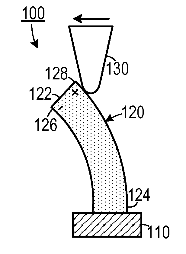
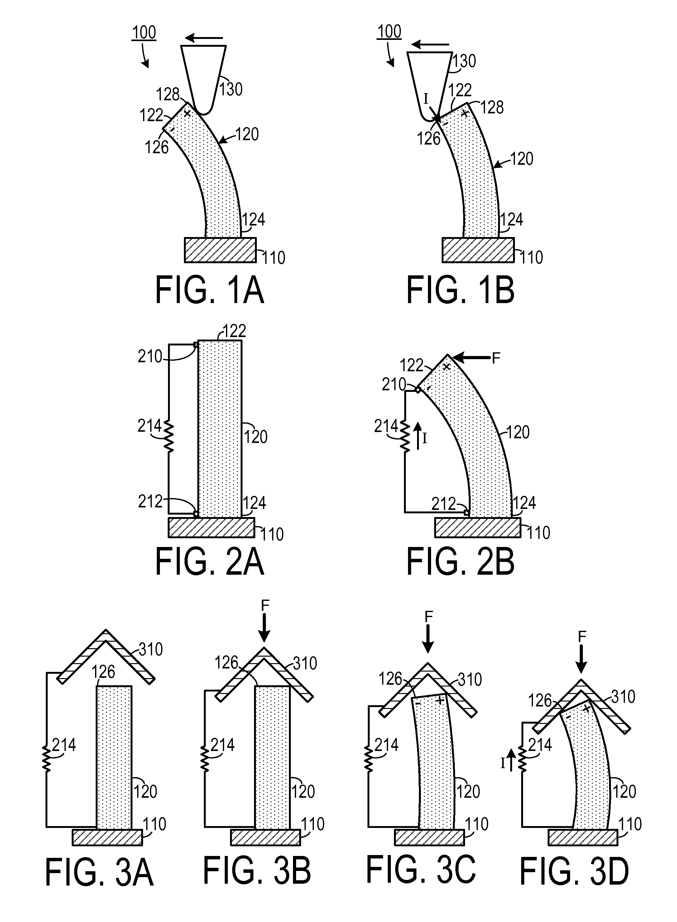
[0062] a generator is shown in FIGS. 2A and 2B, in which a first conductive contact 210 is disposed at the first end 122 and a second conductive contact 212 is disposed at the second end 124. The second conductive contact 212 could be either placed against the semiconductor piezoelectric structure 120 or placed against the substrate 110 if the substrate 110 is made of a conductive material. A load 214 is coupled between the first conductive contact 210 and the second conductive contact 212 so that when a force is applied to the first end 122 in direction F, a current I flows through the load 214.

third embodiment

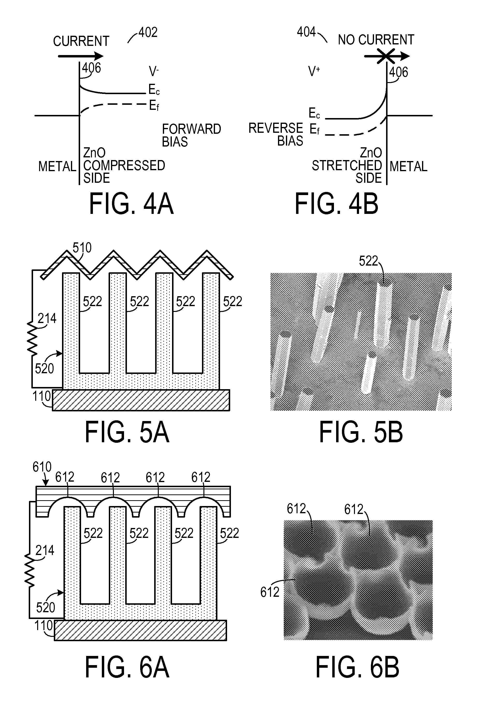
[0063] A third embodiment is shown in FIGS. 3A-3D. In this embodiment, the first conductive contact 310 has an uneven surface. As a downward force is applied to the first conductive contact 310, as shown in FIG. 3B, part of the semiconductor piezoelectric structure 120 makes contact with the first conductive contact 310. This causes the semiconductor piezoelectric structure 120 to bend and a potential difference forms between the two sides of the semiconductor piezoelectric structure 120. Initially, as shown in FIG. 3C, only the positive side of the semiconductor piezoelectric structure 120 is in contact with the first conductive contact 310, which creates a reverse-biased Schottky barrier through which no current flows. However, once the first conductive contact 310 has been pushed down far enough, the negative side of the semiconductor piezoelectric structure 120 makes contact with the first conductive contact 310, thereby forming a forward-biased Schottky barrier and allowing cur...


PUM

PropertyMeasurementUnit
heightaaaaaaaaaa
apex angleaaaaaaaaaa
speedaaaaaaaaaa

Abstract

A semiconducting device includes a substrate, a piezoelectric wire, a structure, a first electrode and a second electrode. The piezoelectric wire has a first end and an opposite second end and is disposed on the substrate. The structure causes the piezoelectric wire to bend in a predetermined manner between the first end and the second end so that the piezoelectric wire enters a first semiconducting state. The first electrode is coupled to the first end and the second electrode is coupled to the second end so that when the piezoelectric wire is in the first semiconducting state, an electrical characteristic will be exhibited between the first electrode and the second electrode.

Description

CROSS-REFERENCE TO RELATED APPLICATION(S) [0001] This application claims the benefit of the following U.S. Provisional Patent Applications: Ser. No. 60 / 813,101, filed Jun. 13, 2006; Ser. No. 60 / 870,700 filed on Dec. 19, 2006; and Ser. No. 60 / 888,408 filed on Feb. 6, 2007, the entirety of each of which is hereby incorporated herein by reference. [0002] This application is a continuation-in-part of U.S. patent application Ser. No. 11 / 608,865, filed Dec. 11, 2006, which is hereby incorporated herein by reference in its entirety.STATEMENT OF GOVERNMENT INTEREST [0003] This invention was made with support from the U.S. government under grant number NCC3-982, awarded by NASA. The government may have certain rights in the invention.BACKGROUND OF THE INVENTION [0004] 1. Field of the Invention [0005] The present invention relates to electronic devices and, more specifically, to nano-scale piezoelectronic devices. [0006] 2. Description of the Prior Art [0007] A Schottky barrier is a metal-sem...

Claims


Application Information

Patent Timeline
Patent Type & Authority Applications(United States)
IPC IPC(8): H01L27/20H01L21/00H01L41/047H01L41/22
CPCB82Y10/00H01L29/0665H01L29/0673H01L29/0676H01L41/1136Y10T29/42Y10S977/811Y10S977/948Y10S977/73Y10S977/724H01L41/22H02N2/18H10N30/306H10N30/01
Inventor WANG, ZHONGLWANG, XUDONGSONG, JINHUIZHOU, JUNHE, JR-HAUN
Owner GEORGIA TECH RES CORP
Why Eureka
Try Eureka