Vapor deposition of silicon dioxide nanolaminates

a technology of silicon dioxide nanolaminates and vapor deposition, which is applied in the direction of chemical vapor deposition coating, coating, material nanotechnology, etc., can solve the problems of slow deposition rate, low productivity, and self-limiting reaction of atomic layer deposition reactions, and achieve the effect of facilitating the production of many devices

Active Publication Date: 2005-05-26
PRESIDENT & FELLOWS OF HARVARD COLLEGE
View PDF41 Cites 335 Cited by
  • Summary
  • Abstract
  • Description
  • Claims
  • Application Information

AI Technical Summary

Benefits of technology

[0038] The practice of the invention facilitates the production of many devices, such as filling trench insulation between transistors in microelectronics, insulating the collars of deep trench capacitors in semiconductor memories, forming insulation between the metal wires in microelectronic devices, sealing low-k semi-porous insulators for electronic devices, making planar waveguides, multiplexers / demultiplexers, micro-electromechanical structures (MEMS), multilayer optical filters, and protective layers against diffusion, oxidation, or corrosion.

Problems solved by technology

One particularly important aspect of this process is that the atomic layer deposition reactions are self-limiting, in that only a certain maximum thickness can form in each cycle, after which no further deposition occurs during that cycle, even if excess reactant is available.
One disadvantage of the existing atomic layer deposition process is its slow deposition rate, at typically less than 0.1 nanometer (nm) per cycle.
These slow rates mean very low productivity, which has meant that atomic layer deposition is too expensive for most potential applications.
Previously known reactions for the atomic layer deposition of silica are particularly slow, requiring more than one minute to complete a reaction cycle.
Another disadvantage of existing atomic layer deposition processes is that the deposited film forms indiscriminately on all exposed surfaces.
While substrate masking may avoid deposition in certain areas, it is not always convenient or possible to integrate masking into the fabrication process.
However, as the sizes of microelectronic devices have become progressively smaller, and integrated circuits are reduced in size to deeper sub-micron dimensions, signal propagation delay, electrical cross talk between conductors, and power consumption are greatly increased due to parasitic capacitance and resistance.
As transistors shrink and the total amount of interconnect wiring increases, delays in that wiring greatly impact circuit performance.
As wires become closer together and operating frequencies climb, cross talk between adjacent lines can degrade signal integrity.
The porous nature of these low-k porous dielectric materials presents special structural challenges when they are integrated into microelectronic devices.
Such diffusion of metal atoms into the porous dielectric layer can lead to excessive leakage currents between other conductive interconnections and lead to a breakdown of the insulating characteristics of the insulating layer.
Standard deposition techniques such as atomic layer deposition that deposit an electrically conductive diffusion barrier onto a low-k or ultra low-k material may result in deposition of conducting material inside the pores and can even introduce electrical short circuits through the low-k insulator.
In addition, another problem that typically results from the use of porous dielectric materials is that openings formed in such materials have relatively rough sidewalls due to the porous nature of the insulating material.
This may create problems in filling the opening with an appropriate conductive metal and undesirable voids, gaps or seams may be created in between the sidewall of the dielectric and the conductive metal.
Another difficulty with currently used methods for filling isolation trenches is that the dielectric is also deposited on top of the flat surfaces between the trenches.

Method used


Image

  • Vapor deposition of silicon dioxide nanolaminates
  • Vapor deposition of silicon dioxide nanolaminates
  • Vapor deposition of silicon dioxide nanolaminates

Examples


example 1

Alternating Layer Deposition of Silica / Alumina Nanolaminate

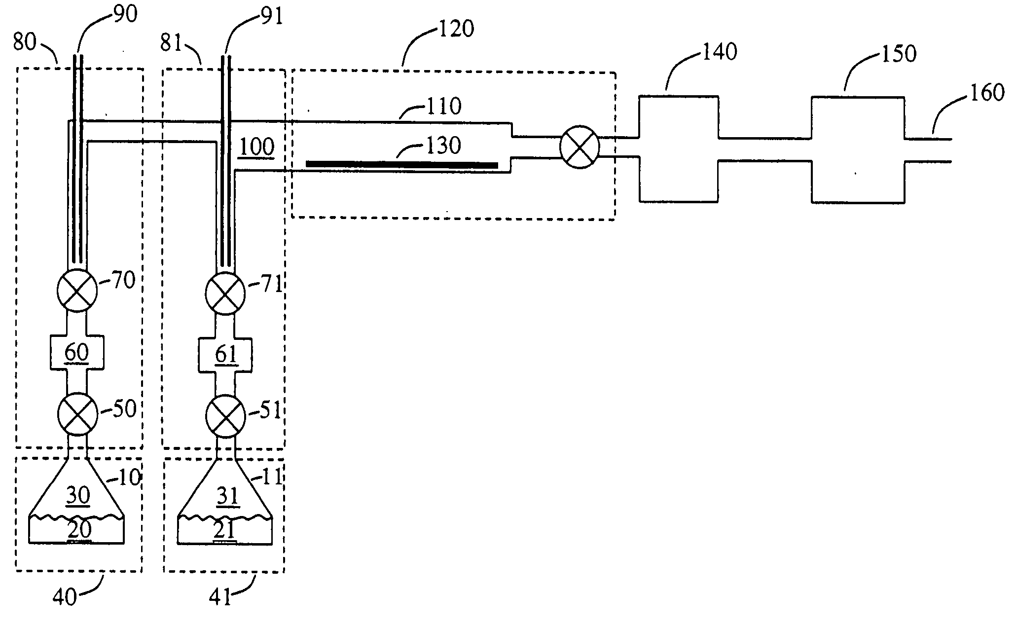
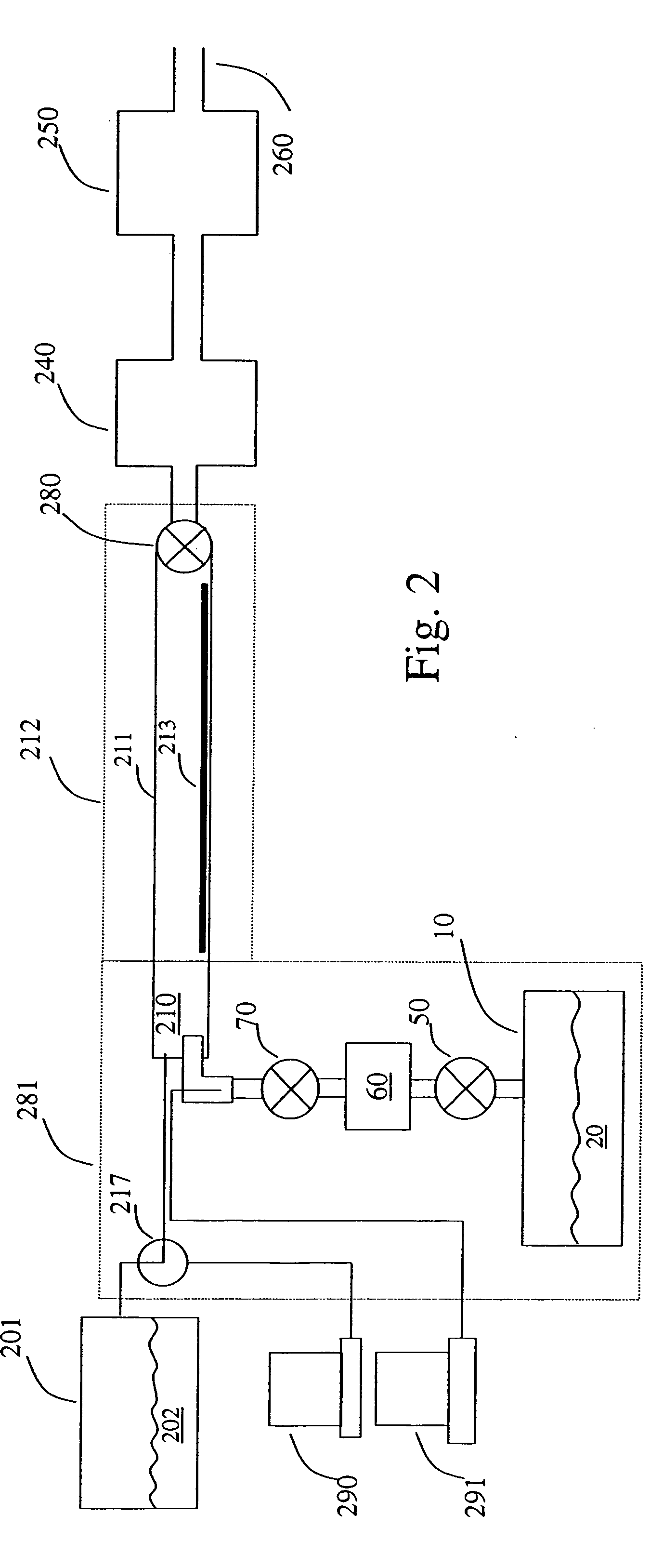
[0102] The apparatus of FIG. 2 was used to deposit silica / alumina nanolaminate films. Tris(tert-butoxy)silanol (“silanol”) was placed in a stainless steel container 201 and heated to 150° C., at which temperature it has a vapor pressure of about 100 Torr. Trimethylaluminum (“TMA”) was held in container 20 at 20° C., so that its vapor pressure was about 14 Torr. A silicon substrate 213 containing holes 7 μm deep and 0.1 to 0.2 μm in diameter was prepared by dissolving its native oxide by placing it in dilute hydrofluoric acid solution for a few seconds. Next the substrate was irradiated by ultraviolet light (e.g. UV mercury lamp) in air until the surface became hydrophilic (about two minutes). Then the substrate 213 was placed in chamber 211 and heated to a temperature of 250° C.

[0103] To deliver pulses of TMA vapor, a three-way valve 217 with inner channels 0.4 mm inner diameter, was opened to TMA vapor for 1 second, durin...

example 2

[0110] Example 1 was repeated, except that the exposure time to silanol vapor was increased from 15 seconds to 90 seconds. Identical results were obtained, showing that the chemical reactions of the silanol were completed within 15 seconds.

example 3

[0111] Example 1 was repeated, except that 100 cycles were used instead of 4 cycles. A film with a uniform total thickness of 1.2 μm (1200 nm) was obtained. This result demonstrated that consistent layers of 12 nm thickness were deposited per cycle for at least 100 cycles.


PUM

PropertyMeasurementUnit
thicknessaaaaaaaaaa
thicknessaaaaaaaaaa
thicknessaaaaaaaaaa

Abstract

This invention relates to materials and processes for thin film deposition on solid substrates. Silica/alumina nanolaminates were deposited on heated substrates by the reaction of an aluminum-containing compound with a silanol. The nanolaminates have very uniform thickness and excellent step coverage in holes with aspect ratios over 40:1. The films are transparent and good electrical insulators. This invention also relates to materials and processes for producing improved porous dielectric materials used in the insulation of electrical conductors in microelectronic devices, particularly through materials and processes for producing semi-porous dielectric materials wherein surface porosity is significantly reduced or removed while internal porosity is preserved to maintain a desired low-k value for the overall dielectric material. The invention can also be used to selectively fill narrow trenches with low-k dielectric material while at the same time avoiding deposition of any dielectric on the surface area outside of the trenches.

Description

RELATED APPLICATIONS [0001] This patent application claims priority under 35 U.S.C. § 120 to and is a continuation-in-part of PCT Application No. US03 / 09736, filed Mar. 28, 2003, the contents of which are incorporated by reference, which claims benefit under 35 U.S.C. § 119(e) to U.S. Provisional Patent Application No. 60 / 368,292, filed Mar. 28, 2002 and 60 / 415,617, filed Oct. 2, 2002, the contents of which are incorporated by reference.STATEMENT AS TO FEDERALLY SPONSORED RESEARCH [0002] This invention was made with the support of the United States government under National Science Foundation Grant No. ECS-9975504. The United States may have certain rights in the invention.BACKGROUND OF THE INVENTION [0003] 1. Field of the Invention [0004] This invention relates to materials and processes for thin film deposition, and in particular, selective thin film deposition, on solid substrates. [0005] This invention also relates to methods and materials for making conformal films for fabricat...

Claims


Application Information

Patent Timeline
Patent Type & Authority Applications(United States)
IPC IPC(8): C23C16/42C23C16/04C23C16/40C23C16/44C23C16/455H01L21/31H01L21/316H01L21/469
CPCC23C16/045C23C16/401C23C16/402C23C16/45555C23C16/45525C23C16/45529C23C16/45534C23C16/403B82Y30/00C23C16/40
Inventor GORDON, ROY G.BECKER, JILLHAUSMANN, DENNIS
Owner PRESIDENT & FELLOWS OF HARVARD COLLEGE
Why Eureka
Try Eureka