

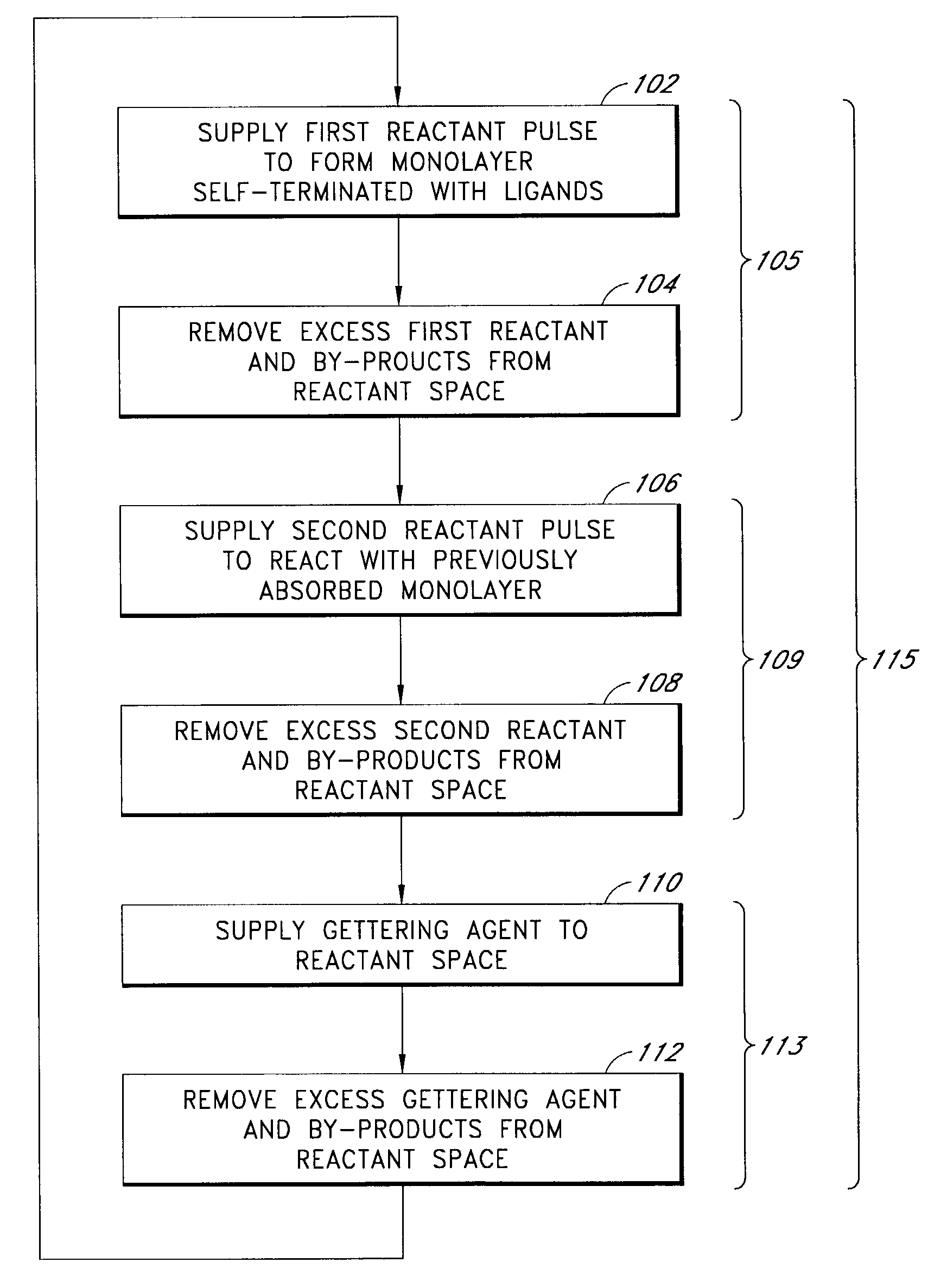
Metal nitride deposition by ALD with reduction pulse
a technology of metal nitride and reduction pulse, which is applied in the direction of ceramic shaping apparatus, special surfaces, electric devices, etc., can solve the problem of surface susceptible to halide attack
- Summary
- Abstract
- Description
- Claims
- Application Information
AI Technical Summary
Problems solved by technology
Method used
Image

Examples
example 1
The Deposition of TiN from TiCl4 and NH3
[0172]A 200-mm silicon wafer coated with PVD copper was loaded into a Pulsar™ 2000™ ALD reactor, commercially available from ASM Microchemistry Oy of Espoo, Finland. The substrate was heated to 400° C. in a flowing nitrogen atmosphere. The pressure of the reactor was adjusted to about 5 mbar by the mass flow controller on the nitrogen line and a vacuum pump. Next, a TiNx layer was grown by ALD from sequential pulses of TiCl4 and NH3 that were separated by inert nitrogen gas.
[0173]One deposition cycle consisted of the following steps:[0174]TiCl4 pulse, for 0.05 s[0175]N2 purge for 1.0 s[0176]NH3 pulse for 0.75 s[0177]N2 purge for 1.0 s
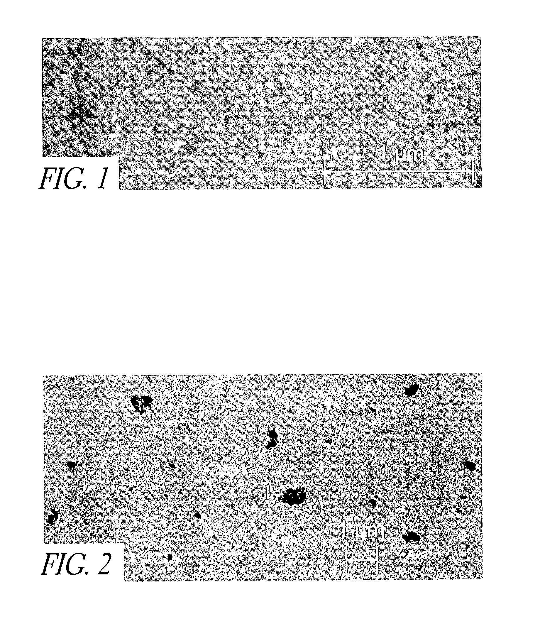
[0178]This cycle was repeated 300 times to form about a 5-nm TiNx film. The growth rate of the TiNx film was about 0.17 Å / cycle. Then the wafer was unloaded from the reactor for analysis. Four-point probe and Energy Dispersive Spectroscopy (EDS) measurements gave a resistivity of 150 μΩcm.
6TiCl4(g)+8NH3(g)→6TiN+2...
example 2
Deposition of WNx from WF6 and NH3
[0181]A 200-mm silicon wafer coated with PVD copper was loaded to a Pulsar™ 2000™ ALD reactor. The substrate was heated to 400° C. in a flowing nitrogen atmosphere. The pressure of the reactor was adjusted to about 5 mbar by the mass flow controller on the nitrogen line and a vacuum pump. Next, a WNx layer was grown by ALD from sequential pulses of WF6 and NH3 that were separated by inert nitrogen gas.
[0182]One deposition cycle consisted of the following steps:[0183]WF6 pulse for 0.25 s[0184]N2 purge for 1.0 s[0185]NH3 pulse for 0.75 s[0186]N2 purge for 1.0 s
[0187]This cycle was repeated 70 times to form about a 5-nm WNx film. The growth rate of the WNx film was about 0.6 Å / cycle. Then the wafer was unloaded from the reactor for analysis.
[0188]Etch damage to the copper film was visible even under an optical microscope because of the nitride process. A lot of HF was evolved from the process (R2) in proportion to the deposited compound. HF may attack...
example 3
Deposition of WNx on SiO2
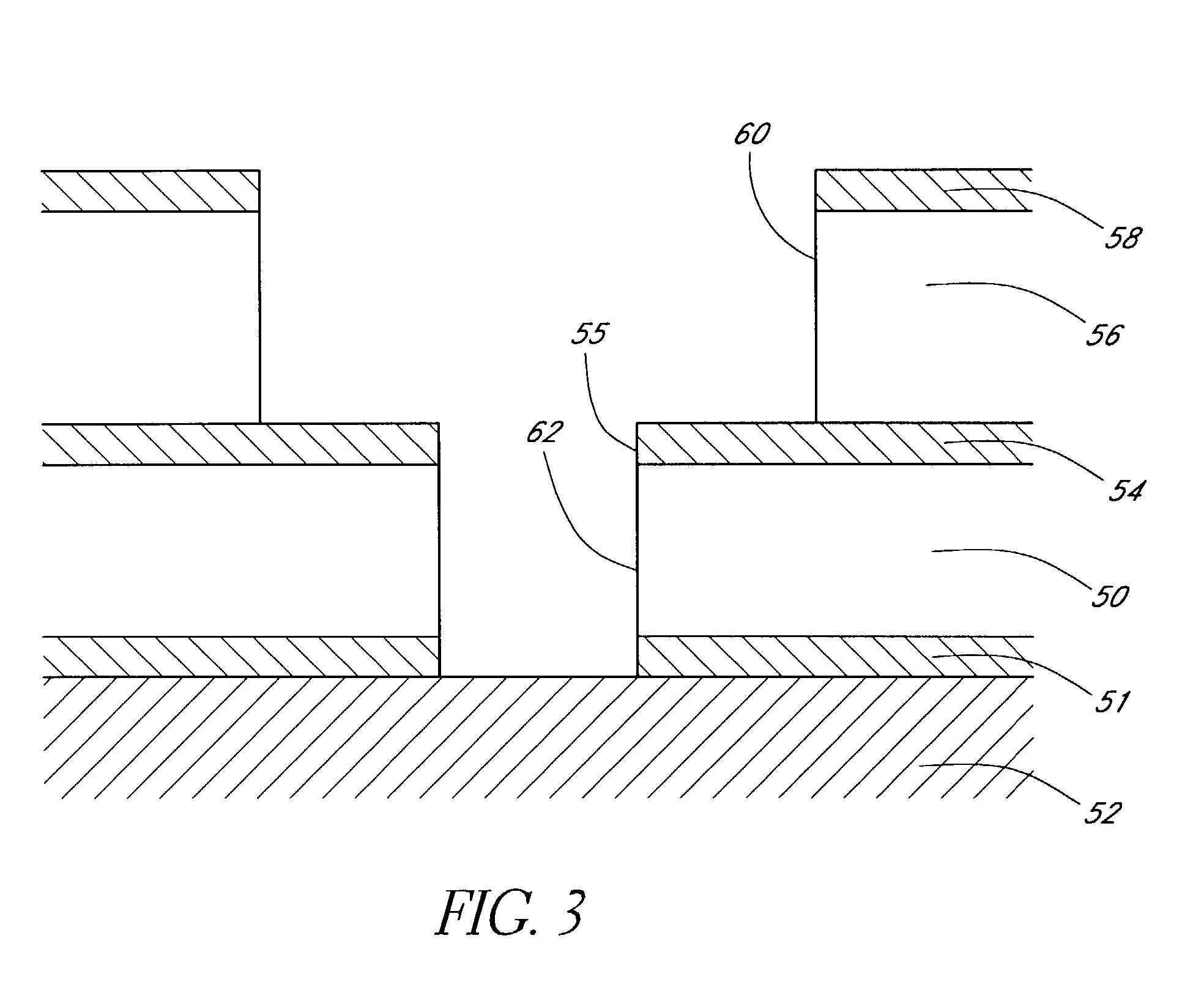
[0189]Tungsten nitride thin film is grown by ALD from sequential pulses of WF6, TEB and NH3 that are separated by inert nitrogen gas pulses.
[0190]One deposition cycle consists of the following steps:[0191]WF6 pulse for 0.25 s[0192]N2 purge for 1.0 s[0193]TEB pulse for 0.05 s[0194]N2 purge for 1.0 s[0195]NH3 pulse for 0.75 s[0196]N2 purge for 1.0 s
[0197]The resulting film on the substrate had rather large resistivity variation across the substrate.
PUM
| Property | Measurement | Unit |
|---|---|---|
| thick | aaaaa | aaaaa |
| temperature | aaaaa | aaaaa |
| temperature | aaaaa | aaaaa |
Abstract
Description
Claims
Application Information