Parasitic particle suppression in growth of III-V nitride films using MOCVD and HVPE

a technology of iiiv nitride and hvpe, which is applied in the direction of polycrystalline material growth, crystal growth process, chemically reactive gas growth, etc., can solve the problems of gan film deposition process, anti-etch layer formation, and additional cost and time of hvp

Inactive Publication Date: 2009-09-08
APPLIED MATERIALS INC
View PDF17 Cites 23 Cited by
  • Summary
  • Abstract
  • Description
  • Claims
  • Application Information

AI Technical Summary

Problems solved by technology

However, the HVPE also has drawbacks for forming GaN and other III-V compound films.
At the very least, the formation of the anti-etch layer will add additional cost and time to the GaN film deposition process.
In addition, the high deposition rates that characterize HVPE processes make them difficult to use with low levels of dopant materials.
Doping steps done after the GaN film is deposited may not provide an adequate concentration or homogeneity of the dopant in the film.
When post-deposition doping is possible at all, it will at the very least add additional cost and time to the GaN film deposition process.
Another major drawback of HVPE is the difficulty of using the process to grow alloys of III-V nitrides, such as aluminum gallium nitride (AlGaN) and indium gallium nitride (InGaN).
But unfortunately generating stable gas precursors for aluminum (e.g., aluminum chloride) and indium (e.g., indium chloride) has proven more difficult than the generation of GaCl.
MOCVD film depositions, however, also have drawbacks.
The slower deposition times make MOCVD a lower throughput and more expensive deposition process than HVPE.
Both approaches have had difficulties.
Scale up to large areas has proved difficult because the GaN must be grown at relatively high pressures (e.g., several hundred Torr), and at these pressures the flow velocity in a large reactor is low, unless the total flow through the reaction is made extraordinarily high.
Consequently, the precursor stream becomes depleted of reactants over a short distance, making it difficult to grow a uniform film over a large area.
Thus, there is competition between the desired film growth and the parasitic particle growth.
In the case of GaN films grown with a trimethylgallium precursor, the film growth rate eventually saturates with respect to the trimethylgallium flow, making it difficult to realize growth rates greater than about 5 μm / hr.
The formation of the parasitic particles can also degrade the optoelectronic qualities of the deposited GaN film.
However, attempts to dilute the precursor gas stream hurt the quality of the III-V film that was deposited.
Unfortunately, high total pressures and high ammonia flows are best for growing AlGaN films with these qualities, but growing these films with the requisite Al content by MOCVD is extremely challenging due to the formation of the parasitic particles.
While the formation of parasitic particles in MOCVD depositions of InGaN is not as pronounced as for AlGaN, it is still significant enough to limit the growth rate of the films.

Method used


Image

  • Parasitic particle suppression in growth of III-V nitride films using MOCVD and HVPE
  • Parasitic particle suppression in growth of III-V nitride films using MOCVD and HVPE
  • Parasitic particle suppression in growth of III-V nitride films using MOCVD and HVPE

Examples


Embodiment Construction

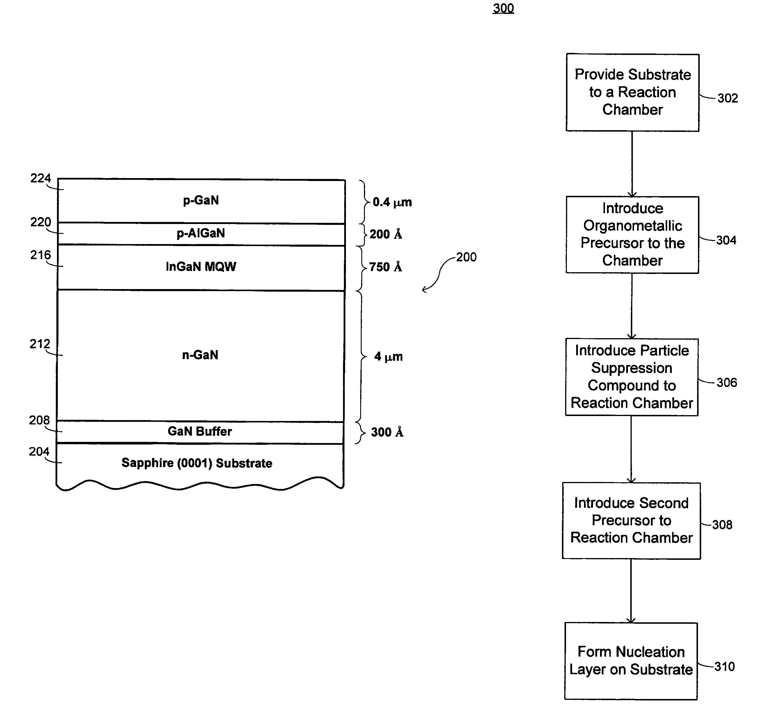
[0036]Systems and methods to suppress the formation of parasitic particles during the deposition of a III-V layer with metal-organic chemical vapor deposition (MOCVD) are described. A particle suppression compound such as a hydrogen halide (e.g., HCl) may be introduced with a Group III metal-organic precursor (e.g., an alkyl gallium precursor) and / or a Group V precursor (e.g., ammonia) to suppress the formation of parasitic III-V particles in the space above a substrate. The partial pressure of the particle suppression compound (or compounds) may be less than the partial pressures of either the Group III or Group V precursors during the deposition of the III-V layer.

[0037]The particle suppression compounds allow the Group III and Group V precursors to be supplied to the reaction chamber at higher partial pressures than would otherwise be possible for growing high quality III-V films with MOCVD. The ability to increase the partial pressures of the film forming precursors without also...


PUM

PropertyMeasurementUnit
temperatureaaaaaaaaaa
thicknessaaaaaaaaaa

Abstract

A method of suppressing parasitic particle formation in a metal organic chemical vapor deposition process is described. The method may include providing a substrate to a reaction chamber, and introducing an organometallic precursor, a particle suppression compound and at least a second precursor to the reaction chamber. The second precursor reacts with the organometallic precursor to form a nucleation layer on the substrate. Also, a method of suppressing parasitic particle formation during formation of a III-V nitride layer is described. The method includes introducing a group III metal containing precursor to a reaction chamber. The group III metal precursor may include a halogen. A hydrogen halide gas and a nitrogen containing gas are also introduced to the reaction chamber. The nitrogen containing gas reacts with the group III metal precursor to form the III-V nitride layer on the substrate.

Description

CROSS-REFERENCES TO RELATED APPLICATIONS[0001]This application is related to co-assigned U.S. patent application Ser. No. 11 / 404,516, by Nijhawan et al, and titled “EPITAXIAL GROWTH OF COMPOUND NITRIDE SEMICONDUCTOR STRUCTURES”, the entire contents which is hereby incorporated by reference for all purposes.BACKGROUND OF THE INVENTION[0002]Group III-V semiconductors are increasingly being used in light-emitting diodes (LEDs) and laser diodes (LDs). Specific III-V semiconductors, such as gallium nitride (GaN), are emerging as important materials for the production of shorter wavelength LEDs and LDs, including blue and ultra-violet emitting optical and optoelectronic devices. Thus, there is increasing interest in the development of fabrication processes to make low-cost, high-quality III-V semiconductor films.[0003]One widely used process for making III-V nitride films like GaN is hydride vapor-phase epitaxy (HVPE). This process includes a high-temperature, vapor-phase reaction between...

Claims


Application Information

Patent Timeline
Patent Type & Authority Patents(United States)
IPC IPC(8): H01L21/44
CPCC23C16/303C23C16/4401C30B25/02C30B29/403C30B29/406C30B25/165H01L21/0262H01L21/02381H01L21/02403H01L21/0242H01L21/02458H01L21/0254H01L21/02378
Inventor BOUR, DAVIDSMITH, JACOB W.NIJHAWAN, SANDEEPWASHINGTON, LORI D.EAGLESHAM, DAVID
Owner APPLIED MATERIALS INC
Why Eureka
Try Eureka