

Graphene film as transparent and electrically conducting material
a graphene film, transparent technology, applied in the direction of non-metal conductors, conductors, metal/alloy conductors, etc., can solve the problems of high-temperature sputtering, inability to achieve the right combination of sheet conductance and transparency, and the indium component of ito is rapidly becoming a scarce commodity
- Summary
- Abstract
- Description
- Claims
- Application Information
AI Technical Summary
Benefits of technology
Problems solved by technology
Method used
Image

Examples
first embodiment
Graphene Flakes
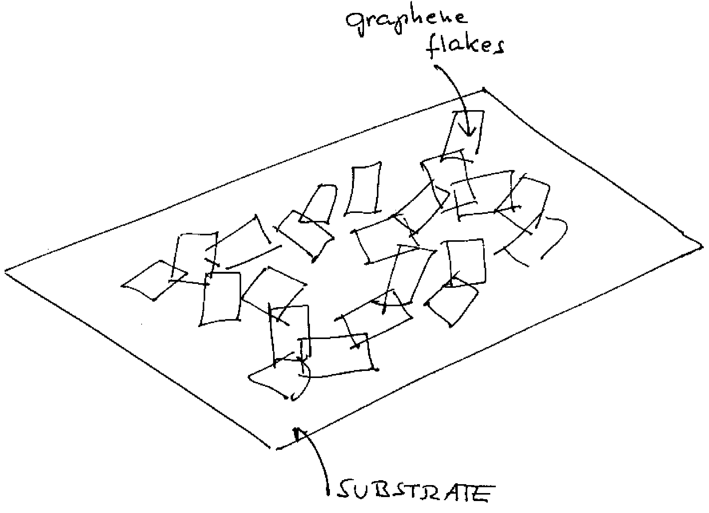
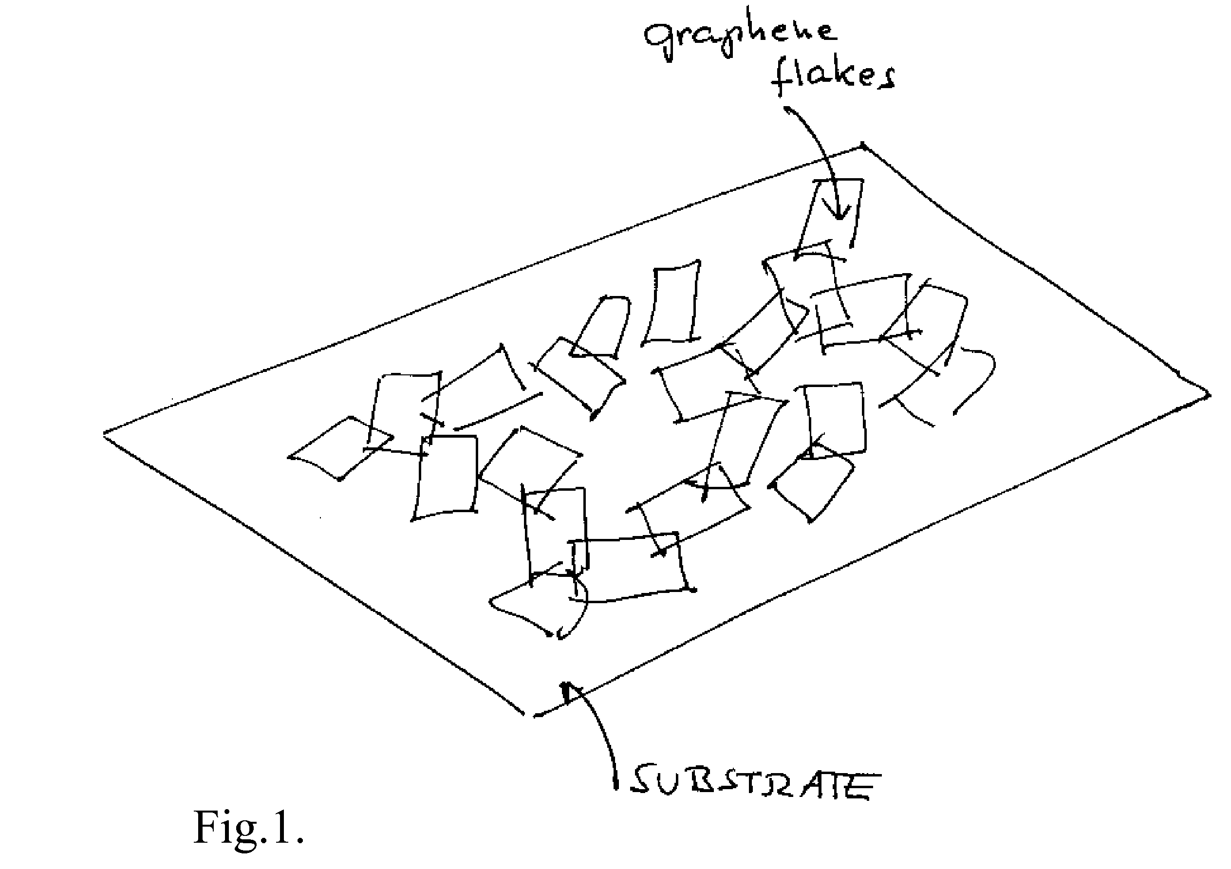
[0019]A first embodiment of the invention is a film formed by an interconnected network of graphene flakes so that there is at least one conduction path across the film.
[0020]Figure one illustrates graphene flakes on a substrate, and figure three provides an SEM image of a graphene flake on a substrate.
[0021]First, commercially available graphene flakes are obtained. The graphene flakes can be treated depending on the desired transparency and conductivity of the resulting films. Examples of preparation steps that can be used to tailor the properties of the resulting films include, but are not limited to, thinning the graphene flakes or doping the graphene flakes. After the graphene flakes have been properly prepared, they are dissolved in solvents such as organic solvents such as dichlorobenzene, chloroform, or dimethylformamide. The solvent can include aqueous dispersions with a suitable surfactant as a solubilization agent. The solvent can also include other solubil...
second embodiment
tworks of Graphene Sheets And Carbon Nanotubes
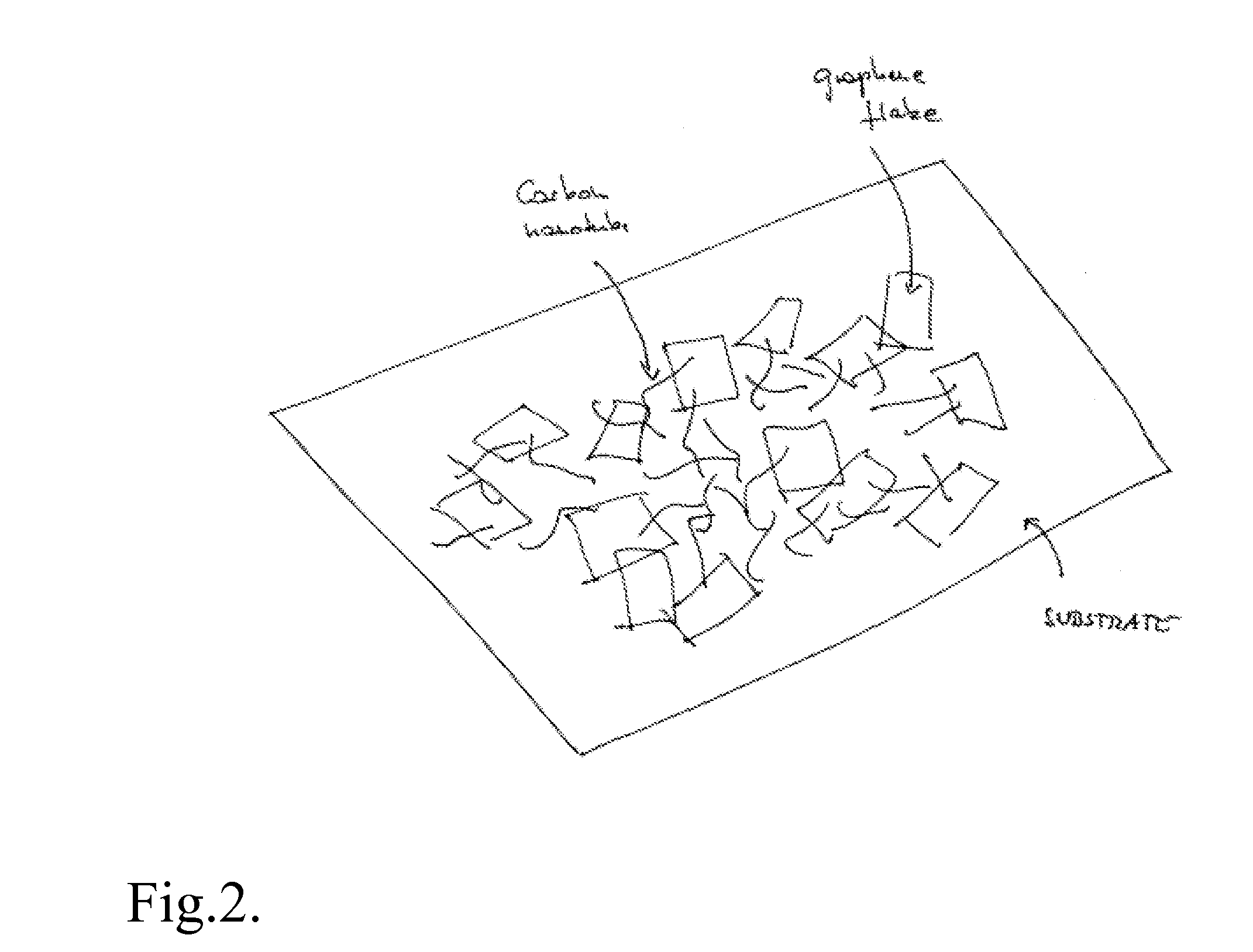
[0025]In another embodiment of the invention, graphene flakes are deposited in combination with other nanostructured materials, in particular carbon nanotubes, so that an interconnected graphene and nanotube layer provides electrical conduction. Figure two is an illustration of a graphene flake—carbon nanotube network, and figure four is an SEM image of a graphene flake—carbon nanotube network.
example
[0026]A graphene flake-carbon nanotube composite was fabricated by repeating the method for the fabrication of the graphene films, with the addition of carbon nanotubes to the solvent. An interpenetrating network of graphene flakes and carbon nanotubes also leads to a network that is 80% transparent and 2 kOhms / sq or 65% and 1 kOhm / sq, where the optical transmission spectra for a 1 kOhm / sq sample is shown in FIG. 5.
PUM
| Property | Measurement | Unit |
|---|---|---|
| optical transparency | aaaaa | aaaaa |
| semi-transparent | aaaaa | aaaaa |
| dc conductivity | aaaaa | aaaaa |
Abstract
Description
Claims
Application Information