Nanogap sensor and method of manufacturing the same
a technology of nano-electrodes and sensors, which is applied in the field of nano-electrodes, can solve the problems of low system resolution and difficulty in forming nano-electrodes, and achieve the effect of easy manufacturing
- Summary
- Abstract
- Description
- Claims
- Application Information
AI Technical Summary
Benefits of technology
Problems solved by technology
Method used
Image
Examples
Embodiment Construction
[0034]Reference will now be made in detail to embodiments, examples of which are illustrated in the accompanying drawings, wherein like reference numerals refer to like elements throughout. In this regard, the present embodiments may have different forms and should not be construed as being limited to the descriptions set forth herein. Accordingly, the embodiments are merely described below, by referring to the figures, to explain aspects of the present description.
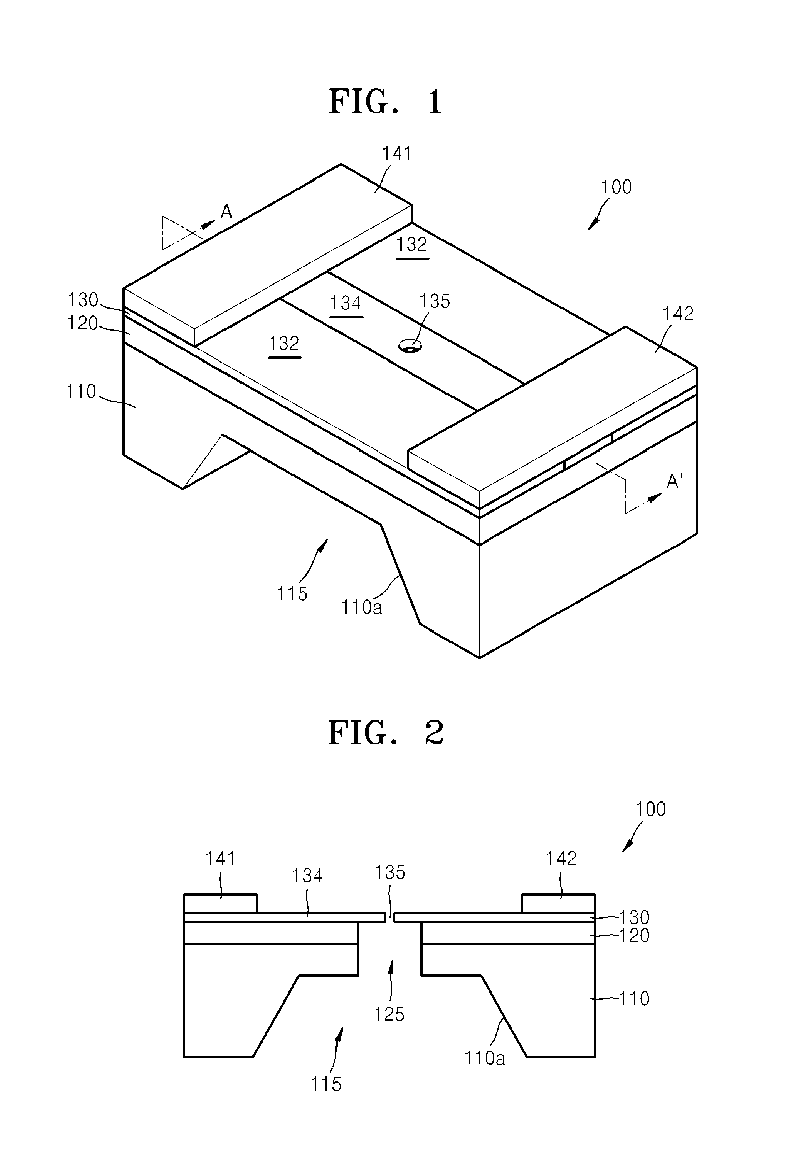
[0035]FIG. 1 is a perspective view of a schematic structure of a nanogap sensor 100 according to an embodiment of the disclosure, and FIG. 2 is a cross-sectional view of the nanogap sensor 100 illustrated in FIG. 1, taken along a line A-A′.
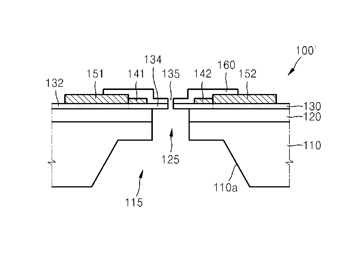
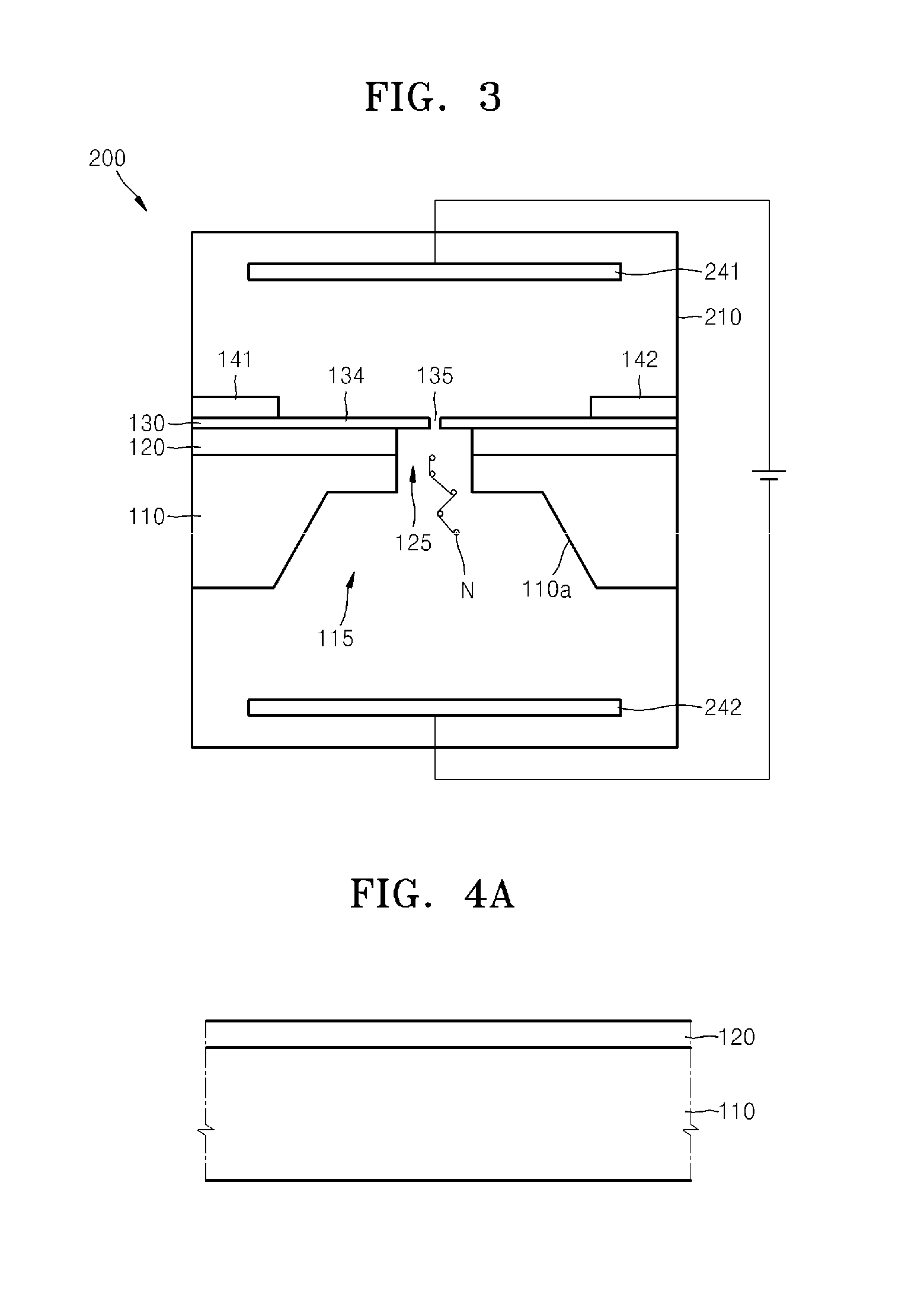
[0036]Referring to FIGS. 1 and 2, the nanogap sensor 100 includes a micropore layer 120 in which a micropore 125 is formed, and a graphene sheet 130 disposed on the micropore layer 120 and including a nanoelectrode region 134 in which a nanogap 135 is formed in a position in which the n...
PUM
 Abstract
Description
Claims
Application Information


