Fuse Structure and Method for Manufacturing Same

a technology of fuse structure and manufacturing method, which is applied in the direction of semiconductor devices, semiconductor/solid-state device details, electrical apparatus, etc., can solve the problems of parasitic capacitance as well as the increase in resistance, corrosion problems that often arise, and circuit breakdown

Active Publication Date: 2008-03-20
INFINEON TECH AG
View PDF33 Cites 98 Cited by
  • Summary
  • Abstract
  • Description
  • Claims
  • Application Information

AI Technical Summary

Problems solved by technology

Since a sealed surface that protects an underlying circuit structure is broken open when destroying the fuse structure, a corrosion problem often arises after destroying the fuse conductive trace.
The corrosion occurring due to the prevailing humidity in the surroundings or due to contacting the semiconductor device with an aggressive substance, for example, to process a surface of the semiconductor device in a further method step, can thereby propagate and/or continue along conductive traces and may even result in a breakdown of the circuit.
The resulting increase in the parasitic capacitances as we

Method used


Image

  • Fuse Structure and Method for Manufacturing Same
  • Fuse Structure and Method for Manufacturing Same
  • Fuse Structure and Method for Manufacturing Same

Examples


first embodiment

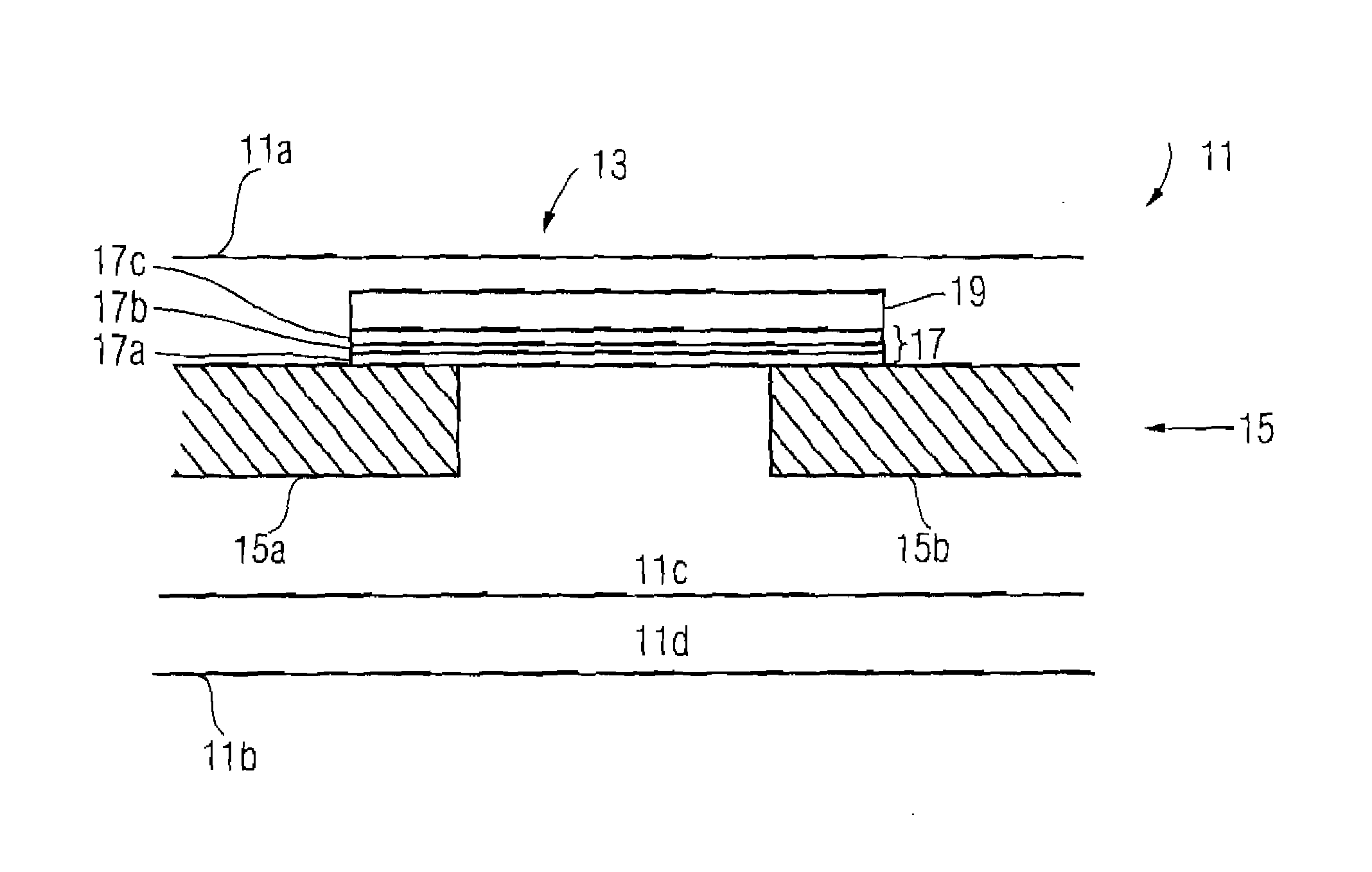
[0022] In the fuse structure 13 according to the present invention, the planar barrier multilayer assembly 17 serves to bring a corrosion process spreading over the fuse conductive trace 19 to a halt, when a hole is created above the fuse conductive trace 19 in the chip 11, for example, in a passivation layer of the same in the vicinity of the first chip surface 11a, as a result of cutting the fuse conductive trace 19. Therefore, the barrier layers 17a, 17b, 17c are manufactured, for example, from a corrosion-resistant material.

[0023] A plurality of the barrier layers 17a-17c are disposed on the fuse structure 13 according to a first embodiment of the present invention between the fuse conductive trace 19 and the metallization layer 15 so that, even in case the corrosion-resistant barrier layers 17a-17c are destroyed by a penetrating aggressive substance, the barrier layer adjacent thereto does not, with a high probability, corrode, and thus an aggressive substance cannot propagate ...

second embodiment

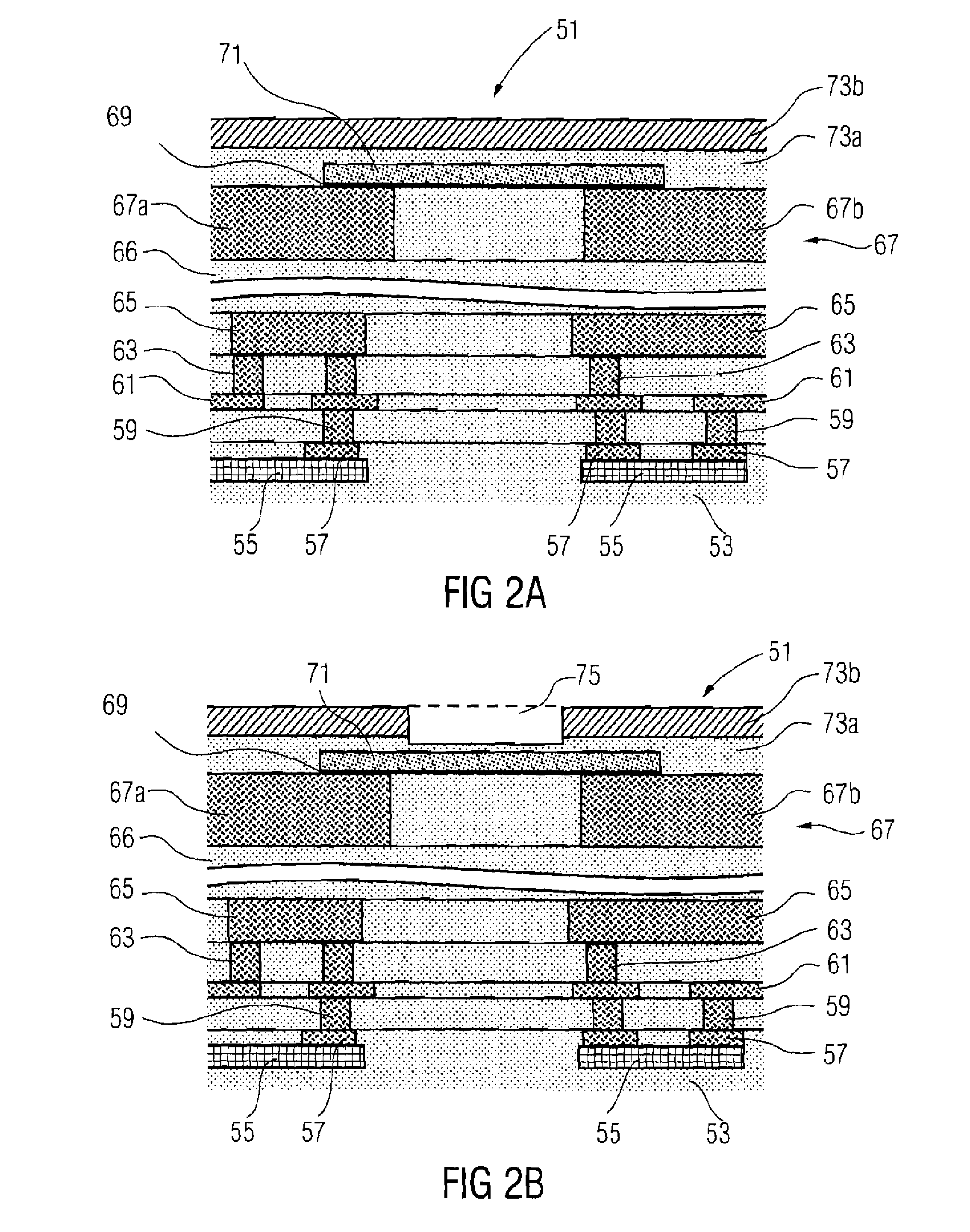
[0037] A design of the fuse structure 51 according to the present invention after cutting the fuse conductive trace 71 is illustrated in FIG. 2c. After the fuse structure 51 shown in FIG. 2b has been irradiated with laser light, a recess 77 is formed in the fuse conductive trace 71 and the planar barrier multilayer assembly 69 as a result of the fuse conductive trace 71 heating. Thus, two portions of the barrier multilayer assembly 69 and the fuse conductive trace 71, which each border one of the two areas 67a, 67b, are separated from each other so that the first area 67a of the metallization layer 67 and the second area 67b of the metallization layer 67 are electrically isolated from each other.

[0038] A width and a thickness of the fuse conductive trace are designed so that the fuse conductive trace 71 and / or the fuse can be cut with an appropriate low laser power, because an irradiation of the fuse structure 51 with a higher laser power could bring about a defect and / or damage in ...

fourth embodiment

[0045]FIG. 5b explains a schematic cross-sectional view of the fuse structure 101 according to the present invention after cutting the fuse conductive trace 71.

[0046] The fuse structure 101 shown in FIGS. 5a-5b serves as a strip line for high-frequency applications and / or RF applications, wherein the high-frequency properties of the strip line implemented in this way are dependent on a distance of the counter-electrode 103 to the fuse conductive trace 71 and the fuse terminals and / or the metallization layer 67. Advantageously, the counter-electrode is disposed in the vicinity of the substrate 53 and away from the passivation 73a, 73b and / or away from the fuse conductive trace 71 so that the counter-electrode 103 is disposed in the semiconductor device shown here only partially so deep down that a probability of damaging when cutting the fuse conductive trace 71 with laser energy and in the corrosion processes starting after that is reduced. Also the counter-electrode 103, like the a...


PUM


Abstract

A fuse structure includes a substrate, a fuse conductive trace disposed closer to a first chip surface than to a second chip surface facing away from the first chip surface, a metallization layer on the substrate disposed on a side of the fuse conductive trace facing away from the first chip surface, and a planar barrier multilayer assembly disposed between the fuse conductive trace and the metallization layer and including multiple barrier layers of different materials, wherein the fuse conductive trace, the metallization layer and the barrier multilayer assembly are arranged such that when cutting the fuse conductive trace and the barrier multilayer assembly, a first area of the metallization layer is electrically isolated from a second area of the metallization layer.

Description

[0001] This application claims priority from German Patent Application No. 10 2006 043 484.6, which was filed on Sep. 15, 2006, and is incorporated herein by reference in its entirety. TECHNICAL FIELD [0002] An embodiment of the present invention relates to a fuse structure (i.e., fusible link structure), and to a method for manufacturing the same. BACKGROUND [0003] In the present application, fuse (fuse=fusible link) means a structure and / or conductive trace in an integrated circuit and / or a semiconductor device that can be destroyed after manufacturing the semiconductor device and / or processing the same at the wafer level. Thus, for example an electrically conductive connection and / or a fuse conductive trace can be cut, thereby effecting a later change in circuit behavior. Destroying and / or cutting is performed by means of an electrical current surge or a laser spike. [0004] The fuse structures are used, for example, for cutting defective parts of a circuit after completion and / or...

Claims


Application Information

Patent Timeline
IPC IPC(8): H01L29/00H01L21/02
CPCH01L23/5258H01L2924/0002H01L2924/00
Inventor BOECK, JOSEFKNAPP, HERBERTLIEBL, WOLFGANGSCHAEFER, HERBERT
Owner INFINEON TECH AG
Why Eureka
Try Eureka