Organic electro-luminescence display device and method of manufacturing the same

a display device and electroluminescence technology, applied in the direction of luminescent screens, discharge tubes, instruments, etc., can solve the problems of reducing the image quality of the organic electroluminescence display device, increasing the number of processes, and leaking current to subpixels adjacent to each other, and achieve excellent image quality characteristics

Active Publication Date: 2008-03-27
LG DISPLAY CO LTD
View PDF3 Cites 3 Cited by
  • Summary
  • Abstract
  • Description
  • Claims
  • Application Information

AI Technical Summary

Benefits of technology

[0011]Embodiments are provided for an organic electro-luminescence display device having charge transport patterns patterned by each subpixel unit and thus having an excellent image quality characteristic.

Problems solved by technology

However, a current may leak to subpixels adjacent to each other due to the HTL and the ETL disposed on the plurality of subpixels.
Such a leakage current generates cross-talk, which consequently, reduces image quality of the organic electro-luminescence display device.
However, in the case where the patterning process is performed on the HTL and the ETL for each pixel, the number of processes increases, and thus manufacturing costs increase.
However, as the photolithography process is successively performed several times, the life of a device may be reduced.

Method used


Image

  • Organic electro-luminescence display device and method of manufacturing the same
  • Organic electro-luminescence display device and method of manufacturing the same
  • Organic electro-luminescence display device and method of manufacturing the same

Examples


Embodiment Construction

[0024]An organic electro-luminescence display device and a method for manufacturing the same will be described below with reference to the accompanying drawings.

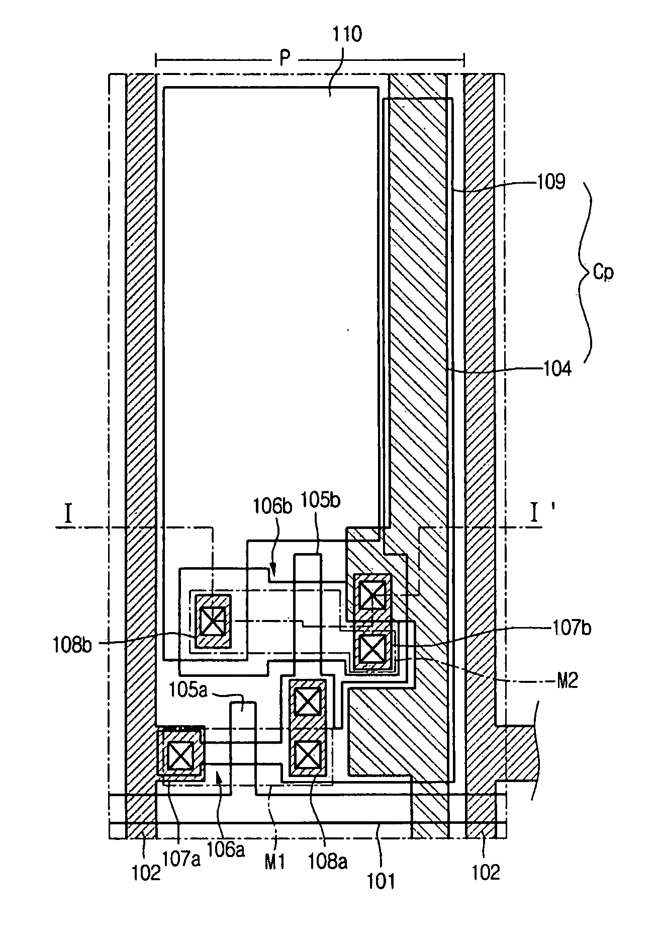
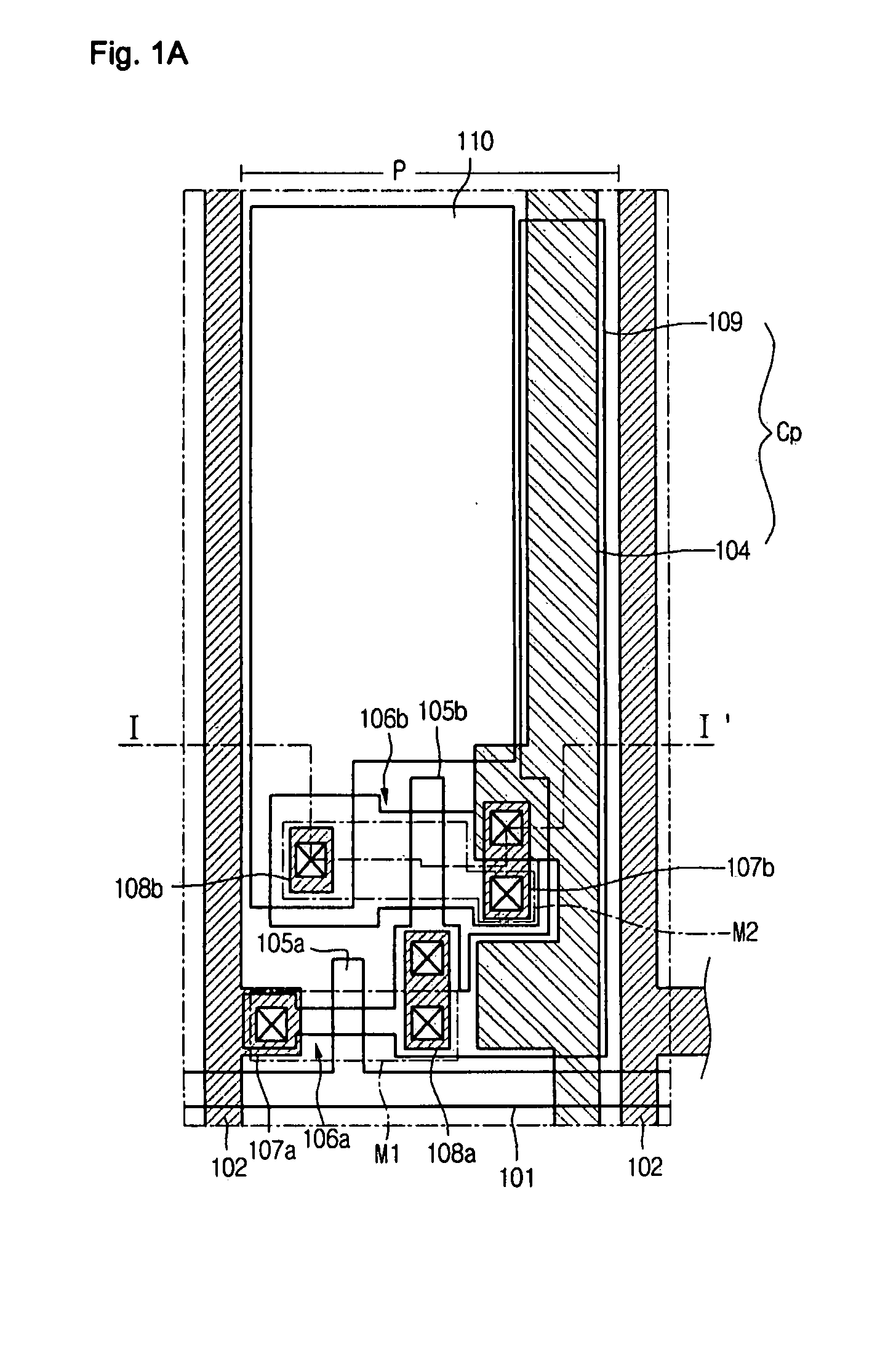
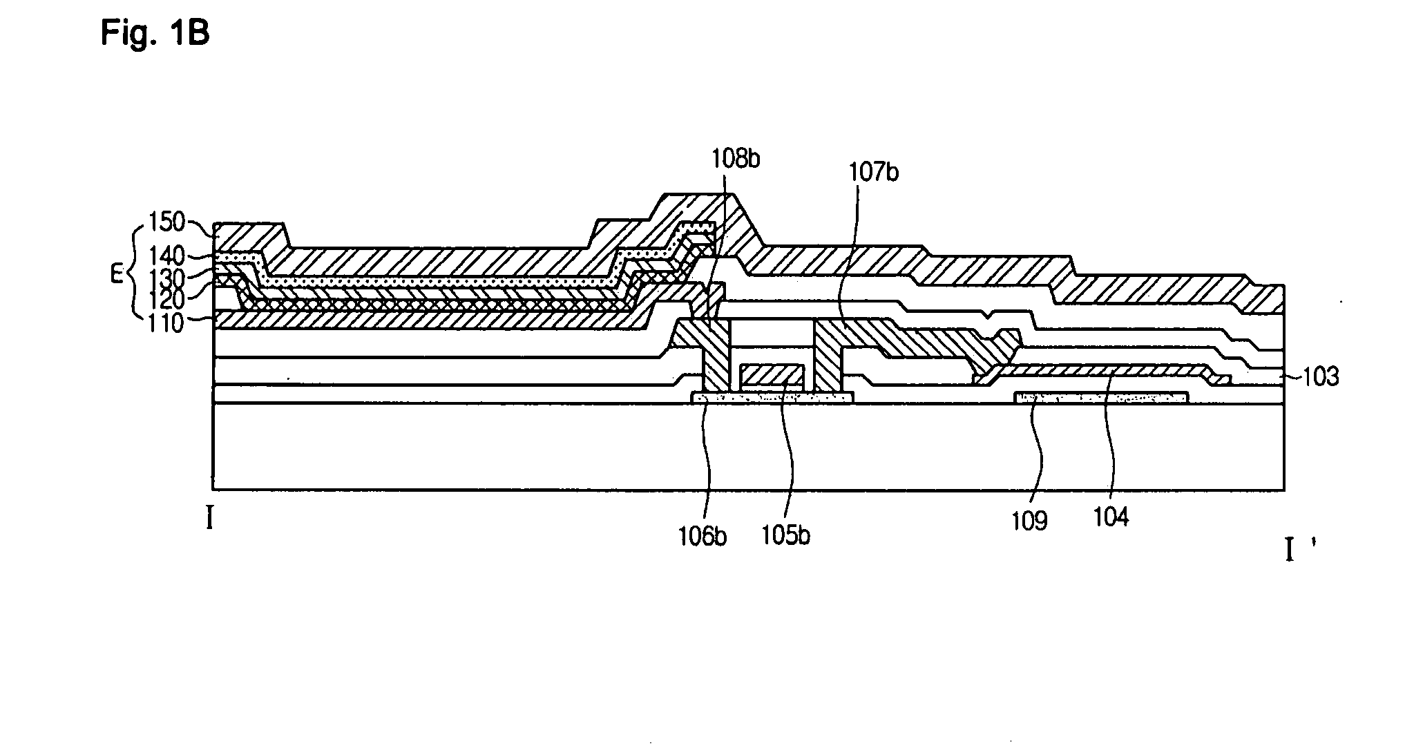
[0025]FIG. 1A is a plan view of an organic electro-luminescence display device according to an embodiment, and FIG. 1B is a cross-sectional view taken along a line I-I′ of FIG. 1A.

[0026]Referring to FIGS. 1A and 1B, the organic electro-luminescence display device includes: a first electrode 110, a first charge transport pattern 120, an organic emission pattern 130, a second charge transport pattern 140, and a second electrode 150 sequentially disposed on a substrate 100.

[0027]In detail, the substrate 100 can be formed of plastics or glass. Particularly, in the case where the organic electro-luminescence display device is a bottom emission type display device transmitting light through the substrate 100, the substrate 100 should be transparent.

[0028]Gate lines 101, and data lines 102 crossing the gate lines 101 with an insula...


PUM

PropertyMeasurementUnit
charge transportaaaaaaaaaa
organicaaaaaaaaaa
charge transportaaaaaaaaaa

Abstract

Provided is an organic electro-luminescence display device. The organic electro-luminescence display device includes: a first electrode, a first charge transport pattern, an organic emission pattern, a second charge transport pattern, and a second electrode. The first charge transport pattern is formed on the first electrode, and the organic emission pattern is on the first charge transport pattern. The second charge transport pattern is formed on the organic emission pattern, and includes an insoluble material. The second electrode is formed on the second charge transport pattern.

Description

PRIORITY INFORMATION[0001]This application claims the benefit of Korean Patent Application No. 2006-92430 filed on Sep. 22, 2006, which is hereby incorporated by reference for all purposes as if fully set forth herein.BACKGROUND[0002]1. Field of the Invention[0003]The present disclosure relates to an organic electro-luminescence display device, and more particularly, to an organic electro-luminescence display device having charge transport patterns patterned by each sub-pixel unit.[0004]2. Description of the Related Art[0005]An organic electro-luminescence display device includes an anode, a cathode, and an organic light emission layer interposed between the two electrodes. The organic electro-luminescence display device realizes an image using the phenomenon that holes and electrodes provided from the anode and the cathode, respectively, recombine in the organic light emission layer to emit light. Therefore, since the organic electro-luminescence display device is a self-luminous d...

Claims


Application Information

Patent Timeline
Patent Type & Authority Applications(United States)
IPC IPC(8): H01L51/54B05D5/12G03C5/00
CPCH01L51/56H01L51/0014H10K71/20H10K71/00H05B33/22H05B33/20
Inventor KIM, YOUNG SOO
Owner LG DISPLAY CO LTD
Why Eureka
Try Eureka