

Flexible TFT device and preparation method thereof
A device and flexible technology, applied in the field of flexible TFT devices and its preparation, can solve the problems of low carrier mobility, achieve low leakage, reduce film cracks, and improve mechanical flexibility
- Summary
- Abstract
- Description
- Claims
- Application Information
AI Technical Summary
Problems solved by technology
Method used
Image

Examples
Embodiment 1
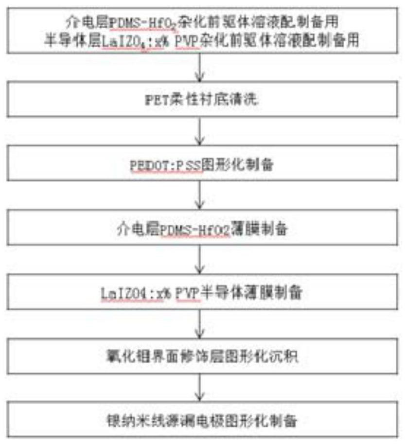
[0056] A flexible TFT device, comprising PET flexible substrate, PI adhesion layer, gate electrode, dielectric layer, PαMS modification layer, semiconductor layer, molybdenum oxide interface modification layer and source-drain electrode layer in sequence, and the gate electrode contains PEDOT:PSS , the dielectric layer contains PDMS-HfO 2 In the hybrid material, the semiconductor layer contains lanthanum indium zinc oxide-polytetravinylphenol hybrid material.
[0057] The preparation method of the flexible TFT device of the present embodiment, such as figure 1 shown, including the following steps:
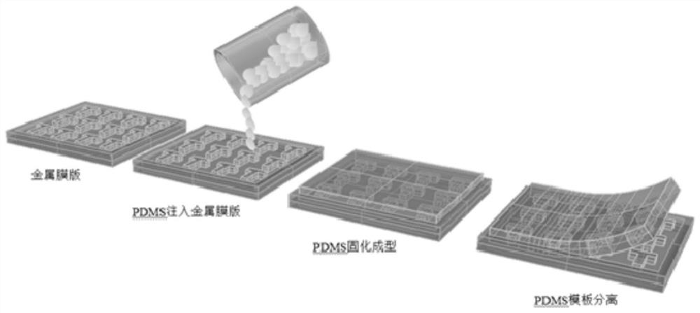
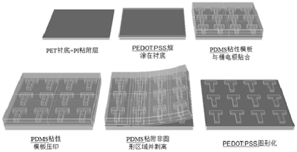
[0058] (1) After tearing off the front protective film of the PET flexible substrate (use a knife to distinguish the front and back), use acetone, isopropanol, ethanol and deionized water to ultrasonically clean it for 4 minutes to remove particulate matter and organic impurities; Dry the water droplets on the surface of PET, and finally place it on a hot plate at 100°C for 8 min...
Embodiment 2
[0072] A flexible TFT device, comprising a PI flexible substrate, a PI adhesion layer, a gate electrode, a dielectric layer, a PαMS modification layer, a semiconductor layer, a TAPC interface modification layer, and a source-drain electrode layer, wherein the gate electrode contains PEDOT:PSS, The dielectric layer contains PDMS-HfO 2 In the hybrid material, the semiconductor layer contains lanthanum indium zinc oxide-polytetravinylphenol hybrid material.
[0073] The preparation method of the flexible TFT device of the present embodiment comprises the following steps:
[0074] (1) After tearing off the front protective film of the PI flexible substrate (use a knife to distinguish the front and back), use acetone, isopropanol, ethanol and deionized water to ultrasonically clean it for 4 minutes to remove particulate matter and organic impurities; Dry the water droplets on the surface of PI, and finally place it on a hot plate at 100°C for 8 minutes to dry;
[0075] (2) Evenly...
Embodiment 3
[0086] A flexible TFT device, comprising PET flexible substrate, PI adhesion layer, gate electrode, dielectric layer, PαMS modification layer, semiconductor layer, molybdenum oxide interface modification layer and source-drain electrode layer in sequence, and the gate electrode contains PEDOT:PSS , the dielectric layer contains PDMS-HfO 2 In the hybrid material, the semiconductor layer contains lanthanum indium zinc oxide-polytetravinylphenol hybrid material.
[0087] The preparation method of the flexible TFT device of the present embodiment comprises the following steps:
[0088] (1) After tearing off the front protective film of the PET flexible substrate (use a knife to distinguish the front and back), use acetone, isopropanol, ethanol and deionized water to ultrasonically clean it for 3 minutes to remove particulate matter and organic impurities; Dry the water droplets on the PET surface, and finally place it on a hot plate at 140°C for 5 minutes to dry;
[0089] (2) Ev...
PUM
 Abstract
Description
Claims
Application Information