
Manufacturing method of display panel

a manufacturing method and display panel technology, applied in the field of display technologies, can solve the problems of high manufacturing cos

Active Publication Date: 2022-08-16
TCL CHINA STAR OPTOELECTRONICS TECH CO LTD
View PDF14 Cites 0 Cited by
  • Summary
  • Abstract
  • Description
  • Claims
  • Application Information

AI Technical Summary

Benefits of technology

This patent simplifies the process of creating patterns on quantum dots by using an alternating electric field between two layers. By adjusting the strength and frequency of the electric field, the quantum dots in a solution layer form a predetermined pattern. This improves productivity and efficiency.

Problems solved by technology

Current patterning techniques of quantum dots are mainly achieved by inkjet printing and photolithography, which have high manufacturing cost and complex preparing processes for pixels that restrict large-scale promotion thereof.

Method used


Image

  • Manufacturing method of display panel
  • Manufacturing method of display panel
  • Manufacturing method of display panel

Examples


Embodiment Construction

[0044]The embodiments of the present disclosure are described in detail hereinafter. Examples of the described embodiments are given in the accompanying drawings, wherein the identical or similar reference numerals constantly denote the identical or similar elements or elements having the identical or similar functions. In the description of the present disclosure, it should be understood that terms such as “upper”, “lower”, “front”, “rear”, “left”, “right”, “inside”, “outside”, “side”, as well as derivative thereof should be construed to refer to the orientation as described or as shown in the drawings under discussion. These relative terms are for convenience of description, do not require that the present disclosure be constructed or operated in a particular orientation, and shall not be construed as causing limitations to the present disclosure.

[0045]Current quantum dot patterning techniques mainly comprise inkjet printing and photolithography. Due to the above two techniques ha...


PUM

PropertyMeasurementUnit
sizesaaaaaaaaaa
thicknessaaaaaaaaaa
electric fieldaaaaaaaaaa

Abstract

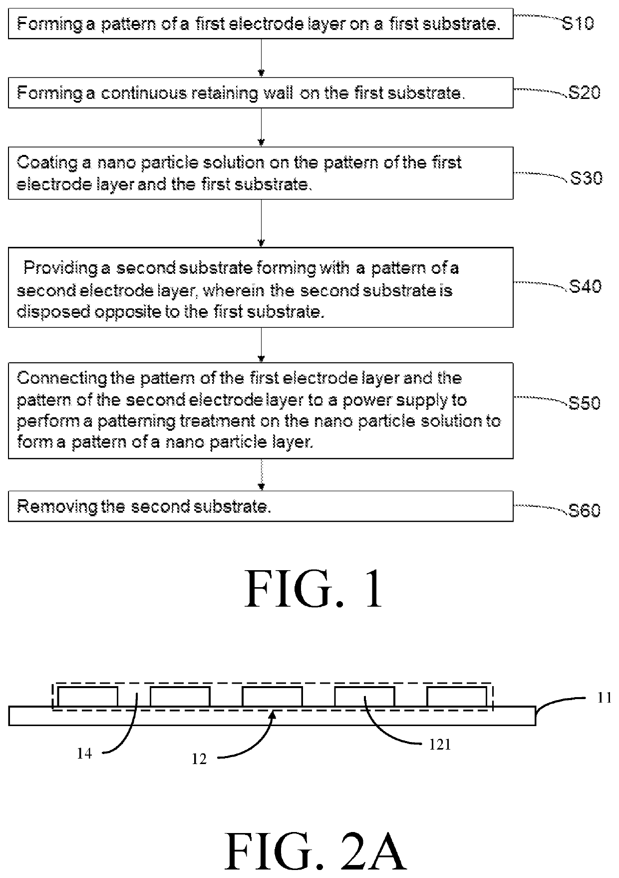
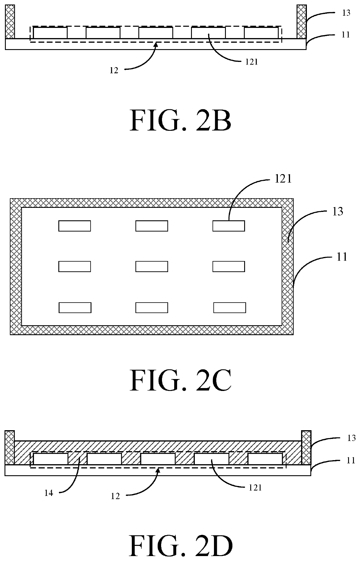
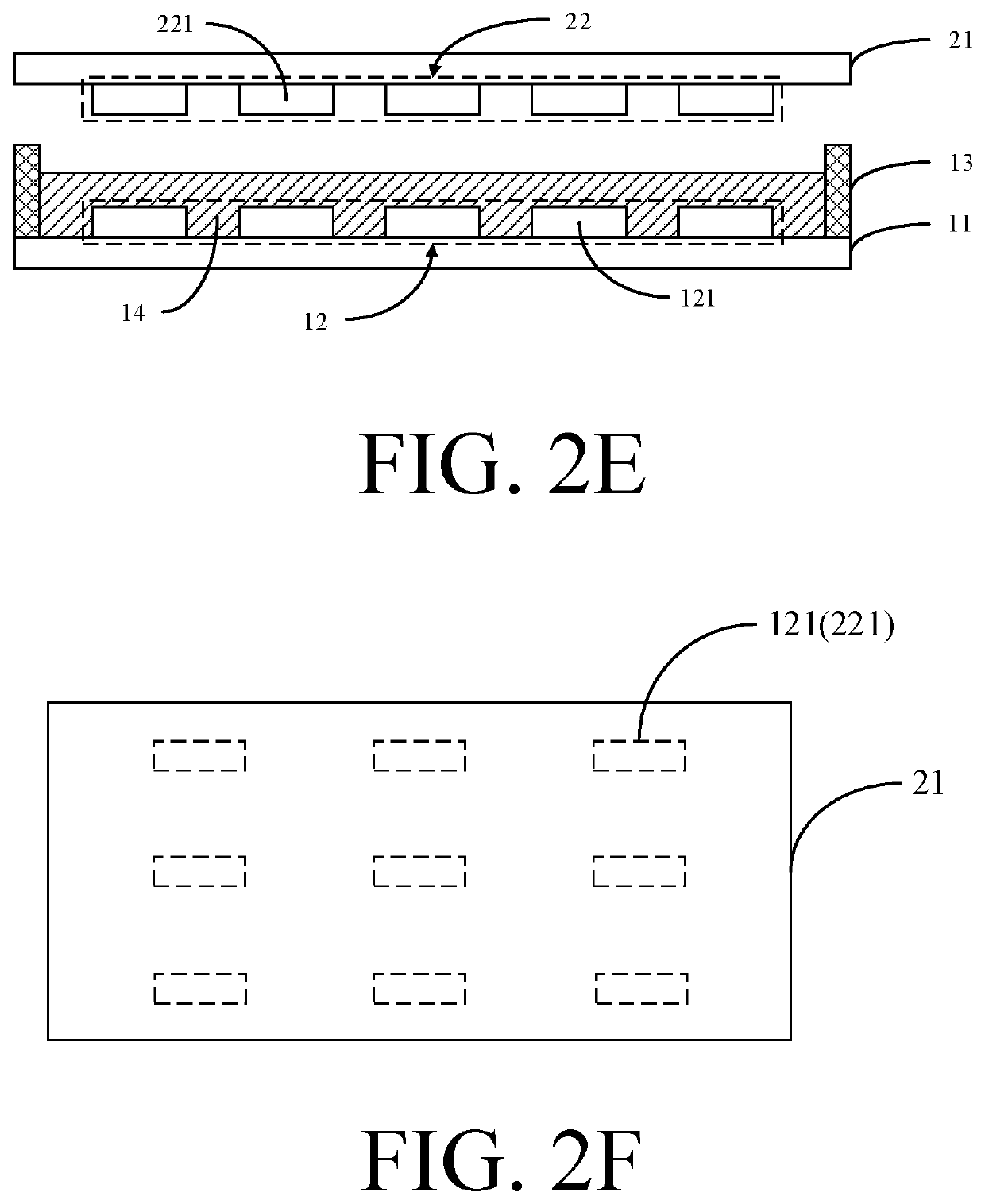
The present disclosure provides a manufacturing method of a display panel which includes forming a pattern of a first electrode layer on a first substrate; coating a nano particle solution on the pattern of the first electrode layer and the first substrate; providing a second substrate formed with a pattern of a second electrode layer, wherein the pattern of the first electrode layer corresponds to the pattern of the second electrode layer; and connecting the pattern of the first electrode layer and the pattern of the second electrode layer to a power supply to perform a patterning treatment on the nano particle solution to make the nano particle solution form a pattern of a nano particle layer.

Description

FIELD OF INVENTION[0001]The present disclosure relates to the field of display technologies, and more particularly, to a manufacturing method of a display panel.BACKGROUND OF INVENTION[0002]Nano materials are structural units having sizes ranging from 1 nm to 100 nm. Due to having volume effect, surface effect, quantum size effect, and macroscopic quantum tunneling effect, nano materials have unique characteristics of melting point, magnetism, optics, thermal conductivity, and electrical conductivity, thereby having important application value in a lot of fields.[0003]Quantum dots are nano materials having high luminous efficiency and narrow emission peak, and are widely used in products of backlights. Current patterning techniques of quantum dots are mainly achieved by inkjet printing and photolithography, which have high manufacturing cost and complex preparing processes for pixels that restrict large-scale promotion thereof.[0004]Therefore, it is necessary to provide a new type o...

Claims


Application Information

Patent Timeline
Patent Type & Authority Patents(United States)
IPC IPC(8): H05K1/09H05K3/06H05K3/24C25D15/00H01L31/00H05K3/28H05K1/02
CPCC25D15/00H05K3/24H05K3/285H05K1/0274H05K3/06H05K2203/0117H05K2203/0776H05K2203/105H05K2203/1105H01L33/505H01L2933/0041H10K59/38H10K71/00H10K59/8722H01L33/50C25D13/22C25D13/18
Inventor ZHAO, JINYANGZHOU, MIAO
Owner TCL CHINA STAR OPTOELECTRONICS TECH CO LTD
Learn More