A method of manufacturing an interconnect structure containing an air gap

A technology of interconnection structure and manufacturing method, applied in semiconductor/solid-state device manufacturing, electrical components, circuits, etc., can solve the problems of small process window and poor sealing integrity, and achieve simplified process, ensure integrity, and large process window. Effect

Active Publication Date: 2017-04-19
SHANGHAI INTEGRATED CIRCUIT RES & DEV CENT
View PDF3 Cites 0 Cited by
  • Summary
  • Abstract
  • Description
  • Claims
  • Application Information

AI Technical Summary

Problems solved by technology

However, the methods of forming the air gap structure in the prior art have the problems of poor sealing integrity and small process window

Method used


Image

  • A method of manufacturing an interconnect structure containing an air gap
  • A method of manufacturing an interconnect structure containing an air gap
  • A method of manufacturing an interconnect structure containing an air gap

Examples


Embodiment 1

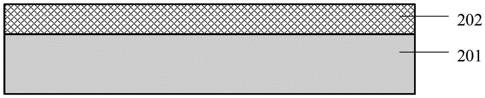
[0033] Please refer to Figure 1A~1I , which is a schematic cross-sectional view of the manufacturing method of this embodiment.

[0034] Please refer to Figure 1A , firstly, a substrate 201 is provided, and the material of the substrate 201 may be silicon, germanium or silicon germanium. In this embodiment, the substrate 201 is a silicon substrate, and the previous process of the substrate 201 has been completed. Then form the first sacrificial layer 202 on the substrate 201, the sacrificial medium of the first sacrificial layer 202 can be SiO2, Si3N4, amorphous silicon material, volatile organic material or polyimide (Polyimide) material with photosensitive properties etc. Preferably, in this embodiment, an amorphous silicon material deposited by plasma enhanced chemical vapor deposition (PECVD) is used as the first sacrificial layer 202 .

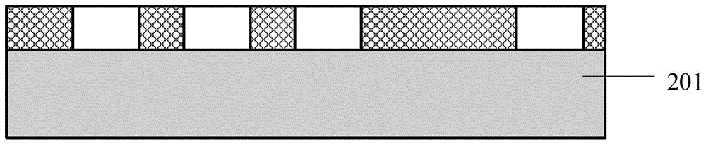
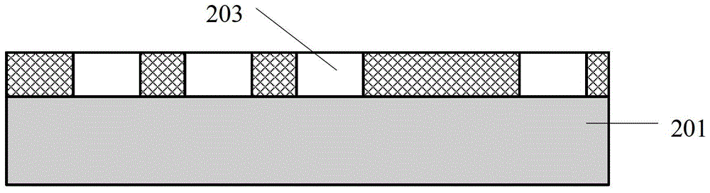
[0035] Please refer to Figure 1B with Figure 1C , which shows a step of performing a single damascene process using the first s...

Embodiment 2

[0044] Please refer to Figure 2A~2J , which is a schematic cross-sectional view of the manufacturing method of this embodiment. The difference from the first embodiment is that the air gap is formed between the metal interconnection structures formed by the double damascene process in this embodiment, which can be used in the first embodiment Completed on the basis of, also can carry out independently, the present invention is not limited to this. Combine below Figure 2A~2J The present embodiment will be described in detail.

[0045] Please refer to Figure 2A , firstly, a substrate 201 is provided, in which a metal interconnection layer 203 is formed, and a dielectric layer 205 is filled between the metal interconnection lines of the metal interconnection layer 203, and the space between the metal interconnection lines and the filling medium can be Air gap 207 is included. The filling medium layer 205 on the surface of the substrate 201 is planarized; preferably, the pl...


PUM


Abstract

The invention discloses a method for manufacturing an interconnection structure containing air gaps. The method includes: forming a first sacrificial layer on a substrate; forming a metal interconnection line in the first sacrificial layer; depositing and etching a second sacrificial layer to form a narrow-end-up peak structure which is connected with a sacrificial medium of the first sacrificial layer; depositing a first medium layer and removing the first medium layer of the upper surface of the second sacrificial layer so as to form a releasing opening at the top of the peak structure; removing sacrificial media of the first sacrificial layer and the second sacrifical layer; and depositing a second medium layer to form the air gaps. By the method, sealing integrity of the air gaps can be guaranteed and the interconnection structure has a larger process window.

Description

technical field [0001] The invention relates to the field of semiconductor integrated circuits, in particular to a method for manufacturing an interconnection structure with an air gap. Background technique [0002] As integrated circuits (Integrated Circuit, IC) continue to shrink according to Moore's Law, the integration level is getting higher and higher, and the various performances of the devices are also demanding higher and higher requirements, among which the back-end process (BEOL, Back End of Line) The introduced resistance-capacitance delay (RC Delay) becomes an important factor that cannot be ignored more and more. The resistance-capacitance time delay is proportional to the resistance of the metal connection and the parasitic capacitance between the fill medium and the metal: [0003] τ∝RC inttot =R(C IMD +C ILD ) Formula 1) [0004] Where R is the resistance of the metal connection, C IMD and C ILD They are the capacitance between metal wirings and the c...

Claims


Application Information

Patent Timeline
Patent Type & Authority Patents(China)
IPC IPC(8): H01L21/768
Inventor 袁超
Owner SHANGHAI INTEGRATED CIRCUIT RES & DEV CENT
Why Eureka
Try Eureka