Method of manufacturing thin film transistor, thin film transistor manufactured by the method, and display device employing the same

A technology for thin film transistors and display devices, which can be used in the manufacture of transistors, semiconductor/solid-state devices, and electric solid-state devices, etc., and can solve problems such as crosstalk, high probability of particle generation, and difficulty in patterning accuracy.

Active Publication Date: 2010-07-28
SAMSUNG DISPLAY CO LTD
View PDF1 Cites 0 Cited by
  • Summary
  • Abstract
  • Description
  • Claims
  • Application Information

AI Technical Summary

Problems solved by technology

[0010] Organic semiconducting materials such as pentacene and polythiophene are difficult and complex to pattern due to their low chemical and optical stability
[0011] Furthermore, even after patterning, such organic semiconductor materials have difficulties in ensuring good patterning accuracy, resulting in a high probability of particle generation, which may cause crosstalk to adjacent OTFTs

Method used


Image

  • Method of manufacturing thin film transistor, thin film transistor manufactured by the method, and display device employing the same
  • Method of manufacturing thin film transistor, thin film transistor manufactured by the method, and display device employing the same
  • Method of manufacturing thin film transistor, thin film transistor manufactured by the method, and display device employing the same

Examples


Embodiment Construction

[0034] Hereinafter, preferred embodiments of the present invention will be described in detail with reference to the accompanying drawings.

[0035] First, refer to Figure 1A to Figure 1F and figure 2 A method of manufacturing a TFT according to a first embodiment of the present invention is described.

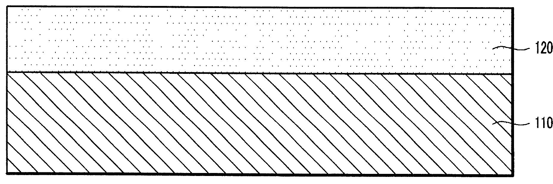
[0036] see Figure 1A , the organic insulating film 120 is coated on the substrate 110 . The substrate 110 may be made of an insulating material such as glass or plastic, or a metallic material such as stainless steel (SUS). Plastics can be polyethylene terephthalate (PET), polyethylene 2,6-naphthalate (PEN), polyethersulfone (PES), polyetherimide, polyphenylene sulfide ( PPS), polyarylate (PAR), polyimide, polycarbonate (PC), polyacrylate, cellulose triacetate and cellulose acetate propionate (CAP), etc. The organic insulating film 120 may be made of negative photoresist.

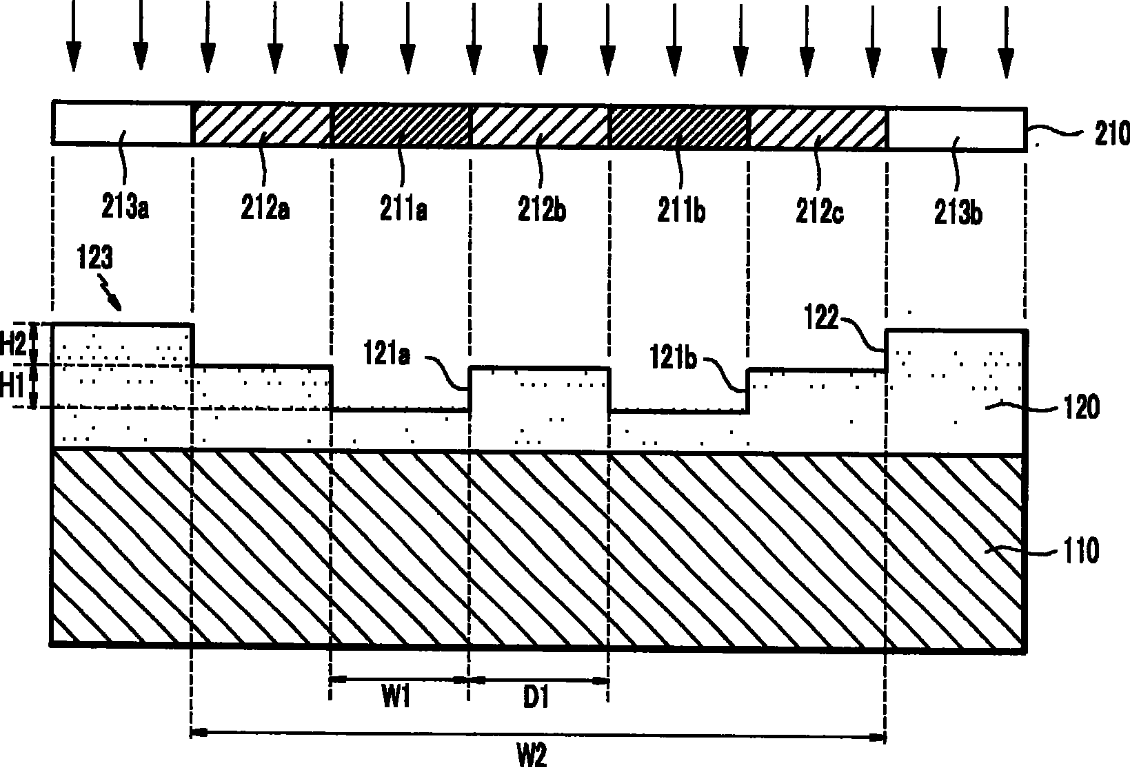
[0037] see Figure 1B , the organic insulating film 120 is exposed using a half-tone mask 210, ...


PUM


Abstract

A method of manufacturing a thin film transistor is capable of enhancing pattern precision of an organic semiconductor layer and simplifying a patterning process. The method includes forming an organic insulating film on a substrate and forming a bank having the first and second concave portions and a third concave portion in the organic insulating film, the third concave portion being formed on the first and second concave portions. The method further includes forming a source electrode and a drain electrode in the first and second concave portions and forming an active layer in the third concave portion, the active layer contacting the source electrode and the drain electrode.

Description

technical field [0001] The present invention relates to a thin film transistor, and more specifically, to a method for manufacturing a thin film transistor by using an organic semiconductor material as an active layer, a thin film transistor manufactured by the method, and a display device using the thin film transistor. Background technique [0002] Display devices such as organic light-emitting displays and liquid crystal displays that are small in thickness and low in operating voltage are being widely used as next-generation display devices, unlike cathode ray tubes (CRTs) that are bulky and high in operating voltage. [0003] In particular, an organic light emitting display is a self-luminous display device in which electrons and holes injected into an organic material through an anode and a cathode are recombined to generate excitons, and light of a certain wavelength is emitted by the energy of the generated excitons. Since the organic light emitting display does not ...

Claims


Application Information

Patent Timeline
Patent Type & Authority Patents(China)
IPC IPC(8): H01L21/336H01L29/786H01L51/40H01L51/05H01L27/15H01L27/32
CPCH10K59/125H10K71/135H10K71/611H10K10/484H10K10/84
Inventor 徐旼徹具在本
Owner SAMSUNG DISPLAY CO LTD
Why Eureka
Try Eureka