
Ink composition for forming transparent conductive film, transparent conductive film, method for producing transparent electrode, and image display device

A technology of transparent conductive film and transparent electrode, which is applied to conductive materials dispersed in non-conductive inorganic materials, cable/conductor manufacturing, photolithographic process exposure devices, etc. , to prevent short circuit, improve curing reactivity and excellent scratch resistance

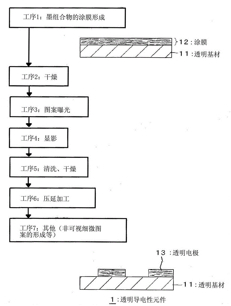
Inactive Publication Date: 2015-12-09
DEXERIALS CORP
View PDF5 Cites 11 Cited by
  • Summary
  • Abstract
  • Description
  • Claims
  • Application Information

AI Technical Summary

Problems solved by technology

However, in these methods, in order to pattern the transparent conductive film, it is first necessary to apply a photoresist on the transparent conductive film and pattern it, thereby increasing the number of steps required for patterning the transparent conductive film.
In addition, a short circuit may occur between the electrodes due to the gap between the electrode patterns formed with the transparent conductive film.

Method used


Image

  • Ink composition for forming transparent conductive film, transparent conductive film, method for producing transparent electrode, and image display device
  • Ink composition for forming transparent conductive film, transparent conductive film, method for producing transparent electrode, and image display device
  • Ink composition for forming transparent conductive film, transparent conductive film, method for producing transparent electrode, and image display device

Examples


Embodiment 1

[0138] First, silver nanowires were fabricated as metal nanowires. The silver nanowires were manufactured by reference ("ACSNano" 2010, Vol.4, No.5, p.2955-2963). The size of the silver nanowires was measured by an electron micrograph as described below, and the average diameter was 30 nm, and the average length was 10 μm.

[0139] Then, the produced silver nanowires (Ag1) and subsequent materials were put into a water / ethanol mixed solvent to manufacture a dispersion in which the silver nanowires were dispersed in the solvent.

[0140] ・Silver nanowire (Ag1): 0.11% by weight

[0141] ・BIOSURFINE-AWP manufactured by Toyo Gosei Kogyo Co., Ltd. represented by the following general formula (II): 0.272% by weight

[0142]・Colored compound (Lanyl Black BGE / C manufactured by Okamoto Dyestuff Co., Ltd. and 2-aminoethanethiol manufactured by Tokyo Kasei Kogyo Co., Ltd. were previously reacted: 0.03% by weight)

[0143] ・Water: 89.588% by weight

[0144] ・Ethanol: 10% by weight

...

Embodiment 2、3

[0153] As a colored compound, instead of Lanyl Black BGE / C manufactured by Okamoto Dyestuff Co., Ltd., DEN manufactured by Sino Co., Ltd. (Example 2) or LA1920 manufactured by Taoka Chemical Industry Co., Ltd. (Example 3) was used, and it was the same as in Example 1. to make transparent electrodes.

Embodiment 4、5

[0155] A transparent electrode was produced in the same manner as in Example 1 except that the integrated light quantity at the time of irradiation was changed to 1 mJ (Example 4) or 5000 mJ (Example 5).


PUM

PropertyMeasurementUnit
lengthaaaaaaaaaa
lengthaaaaaaaaaa
lengthaaaaaaaaaa

Abstract

According to the present invention, for a transparent electrode comprising a transparent conductive film using metal nanowires, the number of patterning steps of the transparent conductive film is simplified and the patterning accuracy of the transparent electrode formed by the transparent conductive film is improved. An ink for forming a transparent conductive film to be used in the formation of transparent electrodes having a distance between electrodes of 20 μm or more contains metal nanowires, a photosensitive material, and a solvent. The average length of the metal nanowires is up to 1.5 times the distance between electrodes.

Description

technical field [0001] The present invention relates to a transparent conductive film containing metal nanowires, an ink composition forming the transparent conductive film, a method for producing a transparent electrode using the ink composition, and an image display device including the transparent conductive film. Background technique [0002] Transparent conductive films are used in image display devices such as liquid crystal displays and plasma displays, and / or touch panels that display images and serve as information input devices. [0003] As a method of forming a transparent conductive film into a predetermined pattern, there is a method of preparing a coating film-forming composition containing a metal nanowire, an amino compound, a (meth)acryloyl compound, a solvent, and a photopolymerizer. This composition is sequentially applied to a substrate, dried, exposed to light through a photomask, and developed (Patent Document 1). There is also a method of forming a tr...

Claims


Application Information

Patent Timeline
Patent Type & Authority Applications(China)
IPC IPC(8): C09D11/52H01B1/00H01B1/22H01B5/14H01B13/00
CPCC09D11/52G02F2202/36G03F7/0047G03F7/008G03F7/0085G03F7/012G02F1/13439H01B1/02G02F1/13338G03F7/20
Inventor 石井康久水野幹久井上纯一金子直人
Owner DEXERIALS CORP
Learn More