

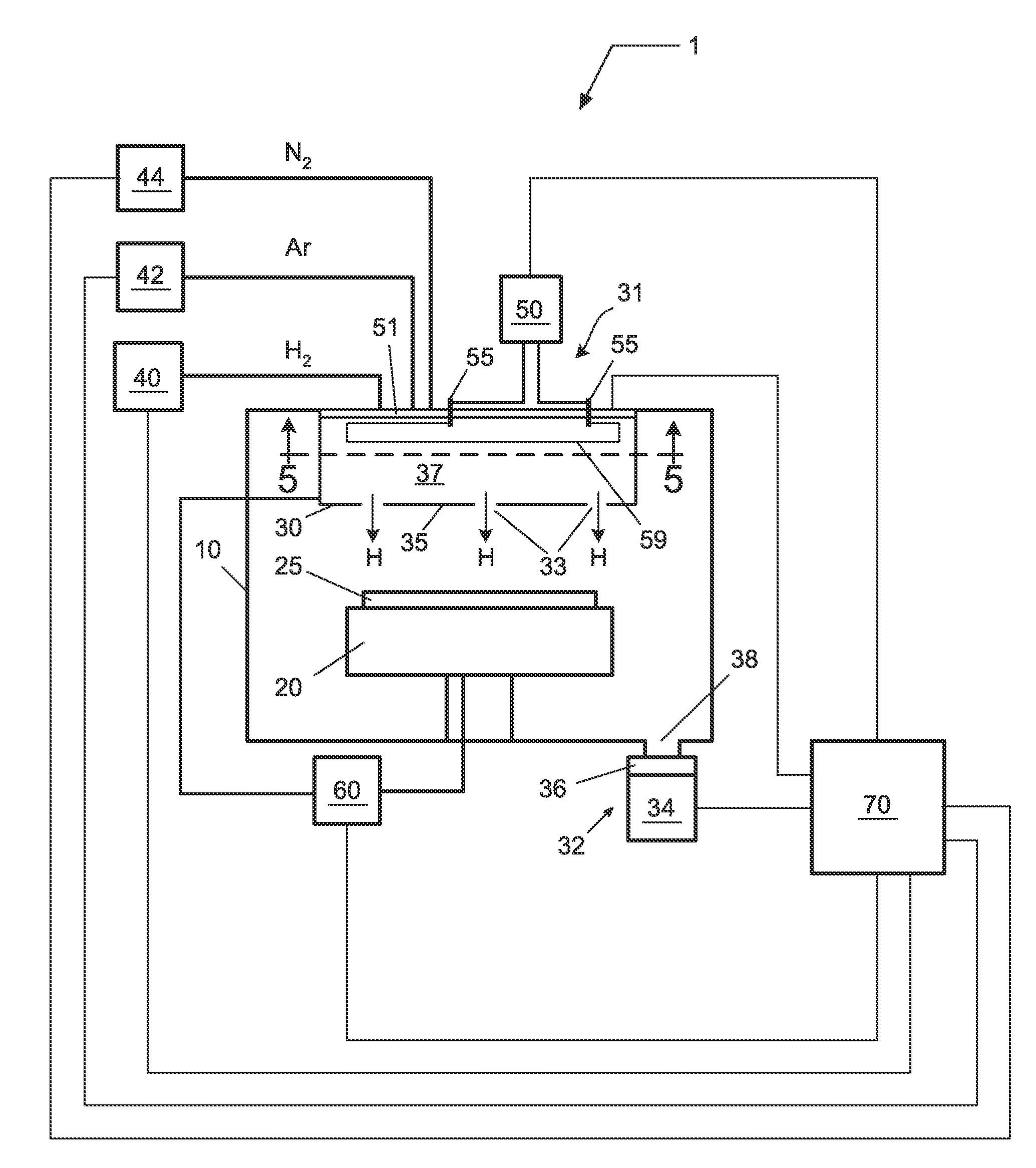
Processing system containing a hot filament hydrogen radical source for integrated substrate processing
a technology of hydrogen radicals and processing systems, which is applied in the direction of coatings, metallic material coating processes, chemical vapor deposition coatings, etc., can solve the problems of increasing signal delays in multilayer interconnect structures and miniaturized semiconductor devices
- Summary
- Abstract
- Description
- Claims
- Application Information
AI Technical Summary
Problems solved by technology
Method used
Image

Examples
Embodiment Construction
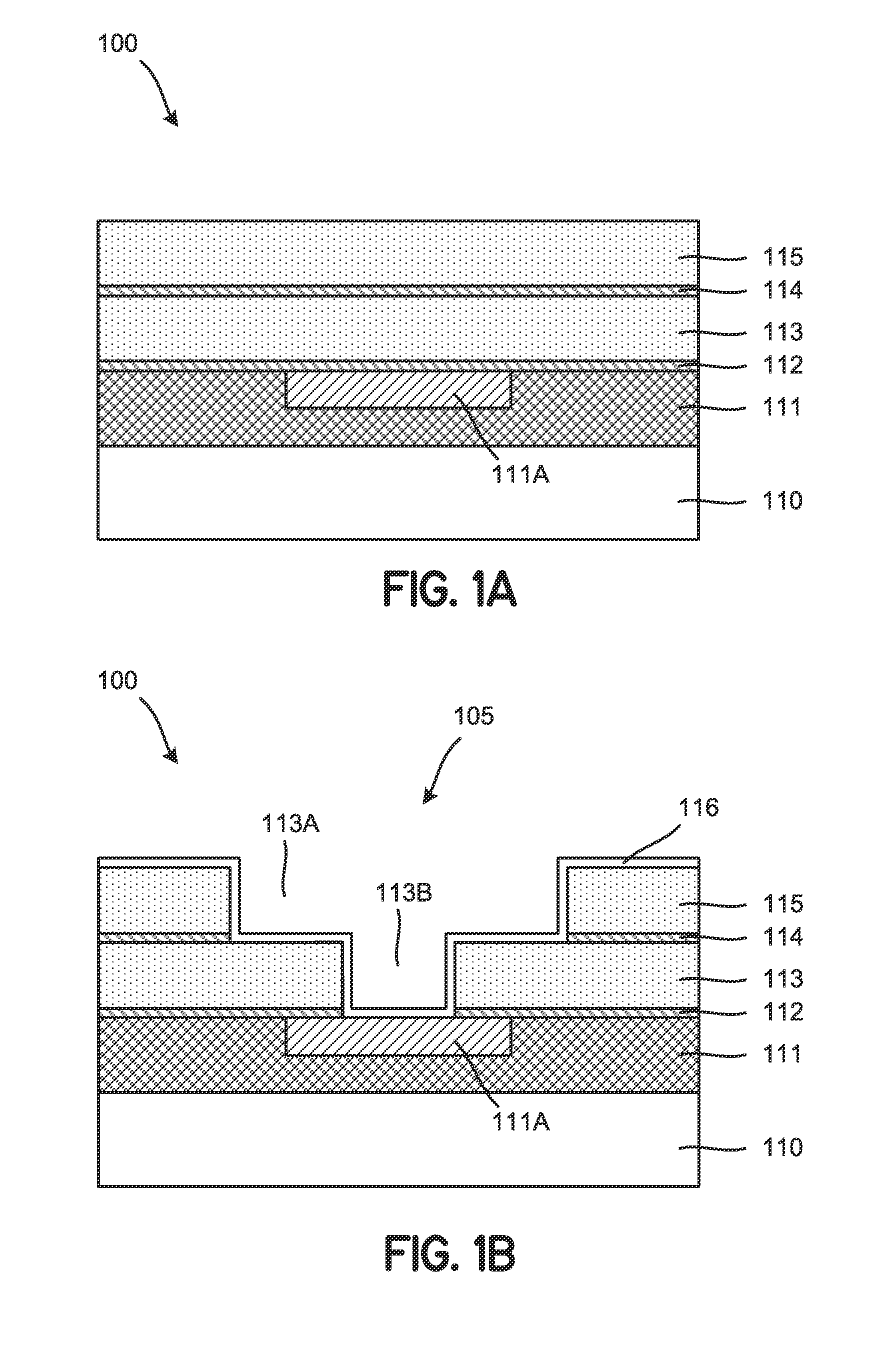
[0021]FIGS. 1A-1C are schematic diagrams of a dual damascene process for forming a multilayer interconnection structure. In FIG. 1A, the structure 100 contains an interconnect pattern 111A of a low-resistance metal such as Cu formed in a SiO2 film 111 on a silicon substrate 110. Furthermore, an etch stop film 112 is formed on the interconnect pattern 111A and the SiO2 film 111, and a low-k dielectric film 113 is formed on the etch stop film 112. Furthermore, an etch stop film 114 is formed on the low-k dielectric film 113, and a low-k dielectric film 115 is formed on the etch stop film 114. The etch stop films 112 and 114 can, for example, contain SiN. The low-k dielectric films 113 and 115 can, for example, contain SiCOH.
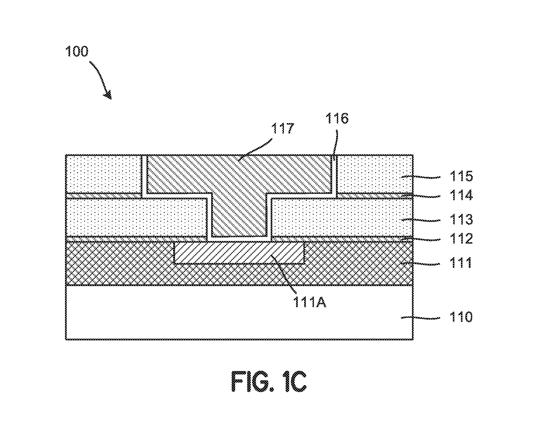
[0022]In FIG. 1B, an etch feature 105 containing a trench 113A and via (hole) 113B are formed in the dielectric films 113 and 115 by a dry etching process, such that the Cu interconnect pattern 111A is exposed at the bottom of the via 113B. As will be described in ...
PUM
| Property | Measurement | Unit |
|---|---|---|
| temperature | aaaaa | aaaaa |
| temperature | aaaaa | aaaaa |
| temperature | aaaaa | aaaaa |
Abstract
Description
Claims
Application Information