Data output control circuit and data output control method

Inactive Publication Date: 2008-04-03
SK HYNIX INC
View PDF12 Cites 59 Cited by
  • Summary
  • Abstract
  • Description
  • Claims
  • Application Information

AI Technical Summary

Benefits of technology

[0013]There is provided a data output control circuit of a semiconductor memory device for controlling a data output in a read operation. The circuit includes: a low frequency mode controller controlling a read command signal in a first operation mode to be output as a first command signal if it is determined to be a high frequency operation through a first CAS latency control sign

Problems solved by technology

As a result, there is a proble

Method used


Image

  • Data output control circuit and data output control method
  • Data output control circuit and data output control method
  • Data output control circuit and data output control method

Examples


Embodiment Construction

[0074]Hereinafter, preferred embodiments of the present invention will be described in detail with reference to the accompanying drawings.

[0075]FIG. 3 shows a first embodiment of the present invention, which is defined by the appurtenant claims and not by any one or more embodiments described herein. In this embodiment, a data output control varies depending on an operation frequency, so that a data output can be stably controlled over a broad range of frequencies.

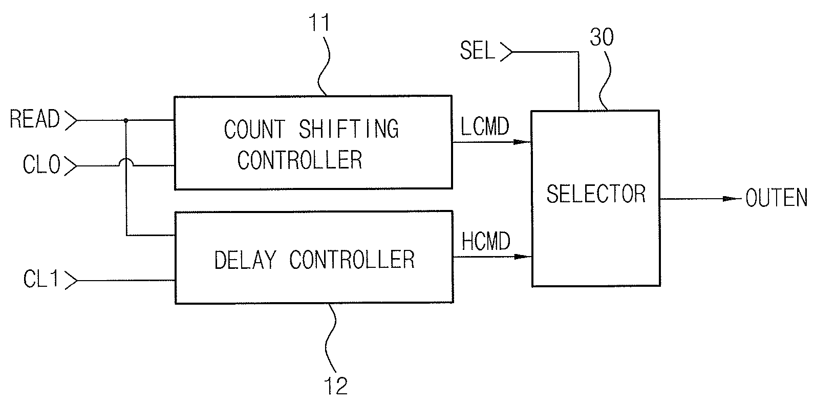
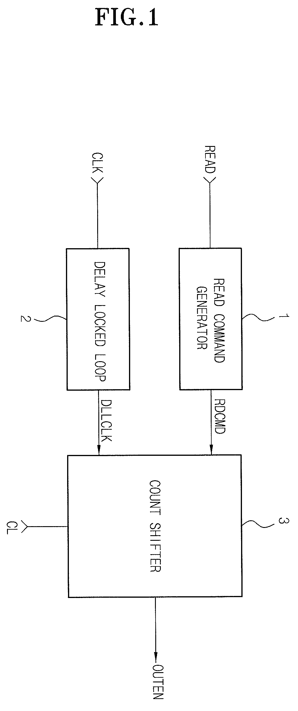
[0076]Specifically, this embodiment of FIG. 3 includes a low frequency mode controller 10, a high frequency mode controller 20 and a selector 30. If a low frequency operation is selected by the CAS latency control signal CL0, the low frequency mode controller 10 controls a read command signal READ to be output as a command signal LCMD for low frequencies in accordance with a low frequency mode operation.

[0077]The CAS latency control signal CL0, is a control signal for low frequencies in which CAS latency CL is bypassed.

[00...


PUM


Abstract

A data output control circuit controls a data output in a read operation. A data output control method includes a count shifting mode and a delay mode and can be used in low and high frequency operations, so that a data output can be stably controlled in a broad frequency range. The data output control circuit includes: a low frequency mode controller a high frequency mode controller and a selector selecting any one of first and second command signals through CAS latency information to be output as a data output control signal.

Description

CROSS-REFERENCE TO RELATED APPLICATIONS[0001]The present application claims priority to Korean patent application number 10-2006-0096616 filed on Sep. 29, 2006, which is incorporated herein by reference in its entirety.BACKGROUND OF THE INVENTION[0002]The present invention relates to a semiconductor memory device, and more precisely to a data output control circuit for controlling a data output in a read operation and a data output control method.[0003]In general, a semiconductor memory device controls the output timing of data read through a data output control circuit so as to transmit data from a memory cell after a read instruction to the outside in a corresponding clock cycle for each CAS latency CL.[0004]Such a conventional data output control circuit may be configured as shown in FIG. 1. Its operation is described below with reference to FIG. 2, which illustrates waveforms of the data output control circuit of FIG. 1 in a case where a CAS latency is 5 (CL=5).[0005]First, a re...

Claims


Application Information

Patent Timeline
IPC IPC(8): G11C7/00
CPCG11C7/1051G11C7/222G11C7/22G11C7/1066G11C7/10
Inventor LEE, HYENG OUK
Owner SK HYNIX INC
Why Eureka
Try Eureka